Microchip / Atmel / ST · Integrated circuit
24LC256 I2C EEPROM
32 KB of non-volatile storage on two wires. The same pinout covers the whole 24Cxx family from 1 Kbit to 512 Kbit.
- Logic level
- 1.7-5.5 V
- Package
- PDIP-8 / SOIC-8 / TSSOP-8
1.Pinout diagram
Highlight a signalhover to preview, click to keep
Pins 1-4
24LC256
Pins 5-8
Pin detail
Hover a pin for its mappings and gotchas. Click to keep it here.
- Logic level
- 1.7-5.5 V
- Package
- PDIP-8 / SOIC-8 / TSSOP-8
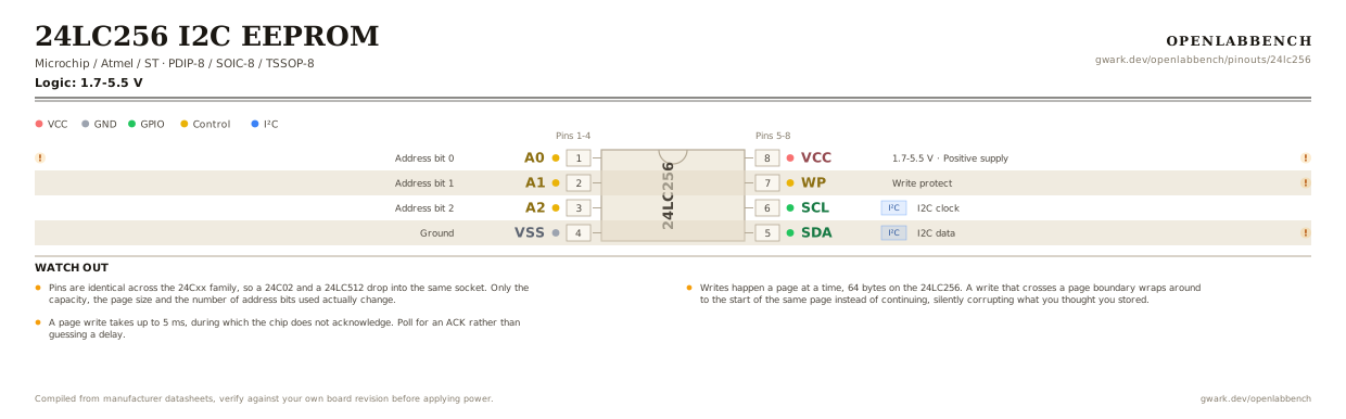
Fig. 1. 24LC256 I2C EEPROM, PDIP-8. Hover or tap a signal to light up every pin that carries it.
2.Watch out
- Pins are identical across the 24Cxx family, so a 24C02 and a 24LC512 drop into the same socket. Only the capacity, the page size and the number of address bits used actually change.
- Writes happen a page at a time, 64 bytes on the 24LC256. A write that crosses a page boundary wraps around to the start of the same page instead of continuing, silently corrupting what you thought you stored.
- A page write takes up to 5 ms, during which the chip does not acknowledge. Poll for an ACK rather than guessing a delay.
- A0 to A2 set the low address bits, giving 0x50 to 0x57. On parts of 512 Kbit and above some of those pins become extra memory address bits instead.
- WP (pin 7) must be grounded to allow writes. Tied high it is read-only, which is useful for calibration data you do not want a bug to overwrite.
- Rated for a million write cycles per page, not per byte. Wear-level anything you update often, or use FRAM such as the FM24CL64, which is pin-compatible and effectively unlimited.
- The cheap DS3231 RTC modules carry an AT24C32 on the same bus, at 0x57. Free storage if you already have one wired up.
3.Minimum circuit
What has to go around the chip before it will run.
| Part | Between | Why |
|---|---|---|
| 4.7 kOhm | SDA (5) to VCC | I2C data is open drain and the bus has no internal pull-ups. |
| 4.7 kOhm | SCL (6) to VCC | The matching pull-up for the clock line. |
| Wire link | A0 (1) to GND | Address bit 0, low. The three address pins must be tied, never left floating. |
| Wire link | A1 (2) to GND | Address bit 1. Tied low here, but it is a real pin: eight of these fit on one bus. |
| Wire link | A2 (3) to GND | Address bit 2, low. All three low gives the base address 0x50. |
| Wire link | WP (7) to GND | Write protect. Held high the part answers reads and silently ignores writes. |
| 100 nF | VCC (8) to GND | Supply decoupling at the pin. |
Writes land a page at a time, 64 bytes on the 24LC256. A write that crosses a page boundary wraps to the start of the same page instead of continuing.
4.Full pin reference
Every pin, alias and mapping. This is the table that prints.
Table 2. Pin assignments.
| Pin | Name | Also called | Functions | Notes |
|---|---|---|---|---|
| 1 | A0 | - | Address bit 0 | Tie high or low, never floating. |
| 2 | A1 | - | Address bit 1 | |
| 3 | A2 | - | Address bit 2 | |
| 4 | VSS | GND | Ground | |
| 5 | SDAI²C | - | I2C data | Open drain. Needs a bus pull-up, 4k7 is typical. |
| 6 | SCLI²C | - | I2C clock | |
| 7 | WP | - | Write protect | Ground to allow writes. High makes the whole device read-only. |
| 8 | VCC1.7-5.5 V | - | Positive supply | 100 nF to ground at the pin. |
Primary sources
Found a wrong pin? The whole board is one file, data/boards/24lc256.json.