Texas Instruments · Integrated circuit
ADS1115 16-Bit ADC
Four single-ended or two differential channels at 16 bits over I2C, with a gain stage and its own reference. What you add when the microcontroller's ADC is not good enough.
- Logic level
- 2-5.5 V
- Package
- VSSOP-10 (DGS) / X2QFN-10 / WCSP
1.Pinout diagram
Highlight a signalhover to preview, click to keep
Pins 1-5
Pins 6-10
Pin detail
Hover a pin for its mappings and gotchas. Click to keep it here.
- Logic level
- 2-5.5 V
- Package
- VSSOP-10 (DGS) / X2QFN-10 / WCSP
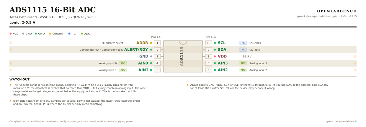
Fig. 1. ADS1115 16-Bit ADC, VSSOP-10 (DGS). Hover or tap a signal to light up every pin that carries it.
2.Watch out
- The full-scale range is not an input rating. Selecting +/-6.144 V on a 3.3 V supply does not let you measure 6 V: the datasheet is explicit that no more than VDD + 0.3 V may reach an analog input. The wide ranges exist so the gain stage can be set below the supply, not above it. This is the mistake that kills these chips.
- ADDR goes to GND, VDD, SDA or SCL, giving 0x48 through 0x4B. If you use SDA as the address, hold SDA low for at least 100 ns after SCL falls or the device may decode it wrong.
- Eight data rates from 8 to 860 samples per second. Slow is not wasted: the lower rates integrate longer and are quieter, and 8 SPS is where the 16 bits actually mean something.
- Four single-ended channels or two differential pairs, not both at once. Differential is the reason to buy this part, because it rejects the common-mode noise that a single-ended reading has no way to see.
- The reference is internal, so readings do not drift with a noisy supply the way a microcontroller ADC referenced to its own 3.3 V rail does.
- ALERT/RDY is open drain and needs a pull-up. It doubles as a conversion-ready strobe, which saves polling the config register in continuous mode.
- The ADS1015 is the same chip at 12 bits and 3300 SPS, pin compatible and register compatible. Code written for one runs on the other with the result shifted four bits.
3.Minimum circuit
What has to go around the chip before it will run.
| Part | Between | Why |
|---|---|---|
| 0.1 uF ceramic | VDD (8) to GND | Supply decoupling at the pin, called for by name in the datasheet's pin table. The reference is derived from this rail. |
| 4.7 kOhm | SDA (9) to VCC | I2C pull-up on SDA. The bus is open drain and cannot pull itself high. |
| 4.7 kOhm | SCL (10) to VCC | I2C pull-up on SCL. One pair per bus, not per device. |
| Address link | ADDR (1) to GND | ADDR tied low, giving 0x48. It is sampled continuously and must not float. |
| 10 kOhmoptional | ALERT/RDY (2) to VCC | Pull-up for ALERT/RDY, which is open drain. Only needed if you use the comparator or the conversion-ready strobe. |
Unused analog inputs should be tied to GND rather than left floating. A high-impedance source wants a capacitor across the input to supply the charge the sampling network takes.
4.Full pin reference
Every pin, alias and mapping. This is the table that prints.
Table 2. Pin assignments.
| Pin | Name | Also called | Functions | Notes |
|---|---|---|---|---|
| 1 | ADDR | - | I2C address select | GND, VDD, SDA or SCL for 0x48 to 0x4B. Four states, not two. |
| 2 | ALERT/RDY | - | Comparator out, Conversion ready | Open drain. Needs a pull-up. Not present on the ADS1113. |
| 3 | GND | - | - | |
| 4 | AIN0ADC | - | Analog input 0 | Must stay between GND - 0.3 V and VDD + 0.3 V, whatever gain you select. |
| 5 | AIN1ADC | - | Analog input 1 | Pairs with AIN0 for a differential reading. |
| 6 | AIN2ADC | - | Analog input 2 | ADS1115 only. Not connected on the ADS1113 and ADS1114. |
| 7 | AIN3ADC | - | Analog input 3 | ADS1115 only. Pairs with AIN2. |
| 8 | VDD2-5.5 V | - | - | Also the ceiling on every analog input. |
| 9 | SDAI²C | - | I2C data | |
| 10 | SCLI²C | - | I2C clock |
Looking for a substitute?
Primary sources
Found a wrong pin? The whole board is one file, data/boards/ads1115.json.