Arduino · Dev board
Arduino Nano v3
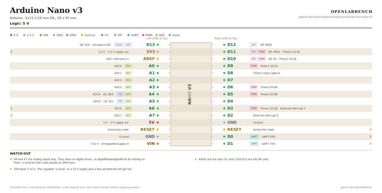
The same ATmega328P as the Uno on a 18 x 45 mm breadboard-friendly footprint, plus two extra analog-only inputs. Orientation below has the USB connector at the top.
- Logic level
- 5 V
- Package
- 2x15 2.54 mm DIL, 18 x 45 mm
1.Pinout diagram
Highlight a signalhover to preview, click to keep
Left (USB at top)
Right (USB at top)
Pin detail
Hover a pin for its mappings and gotchas. Click to keep it here.
- Logic level
- 5 V
- Package
- 2x15 2.54 mm DIL, 18 x 45 mm
Fig. 1. Arduino Nano v3, 2x15 2.54 mm DIL, 18 x 45 mm. Hover or tap a signal to light up every pin that carries it.
2.Watch out
- A6 and A7 are analog inputs only. They have no digital driver, so digitalRead/digitalWrite do nothing on them, a surprise that costs people an afternoon.
- A4/A5 are the only I2C pins; D10-D13 are the SPI pins.
- VIN takes 7-12 V. The regulator is small, so a 12 V supply plus a few peripherals will get hot.
- Clones ship with a CH340 instead of the original FT232RL, which needs a different USB driver but is otherwise interchangeable.
- RESET appears twice on the header, which is handy when the ICSP side is occupied.
- The newer Nano Every, Nano 33 IoT and Nano ESP32 keep this footprint but are 3.3 V parts with different peripherals.
3.Register configuration
Turning a pin on the diagram into a configured pin.
Drive a pin, and read one with a pull-up
avr-libc
#include <avr/io.h>

/* Three registers per port. DDR picks direction, PORT writes the
   output latch, PIN reads the physical pin. */

DDRB  |=  (1 << PB5);          /* PB5 = Arduino D13 = output */
PORTB |=  (1 << PB5);          /* high */
PORTB &= ~(1 << PB5);          /* low  */
PINB  |=  (1 << PB5);          /* writing PIN toggles the output */

DDRD  &= ~(1 << PD2);          /* PD2 = D2 = input */
PORTD |=  (1 << PD2);          /* PORT on an input enables the pull-up */

if (!(PIND & (1 << PD2))) {    /* switch to ground reads 0 when pressed */
}
On an input pin, PORT is the pull-up enable, not an output value. Forget it and a floating pin reads whatever the nearest mains cable is doing.
4.Full pin reference
Every pin, alias and mapping. This is the table that prints.
Table 1. Pin assignments.
| Pin | Name | Also called | Functions | Notes |
|---|---|---|---|---|
| - | D13SPIClock | SCK, PB5 | SPI SCK, On-board LED | |
| - | 3V33.3 V | - | 3.3 V supply out | From the USB bridge, 50 mA at most. |
| - | AREF | - | ADC reference in | |
| - | A0ADC | D14, PC0 | ADC0 | |
| - | A1ADC | D15, PC1 | ADC1 | |
| - | A2ADC | D16, PC2 | ADC2 | |
| - | A3ADC | D17, PC3 | ADC3 | |
| - | A4ADCI²C | D18, SDA, PC4 | ADC4, I2C SDA | |
| - | A5ADCI²C | D19, SCL, PC5 | ADC5, I2C SCL | |
| - | A6ADC | ADC6 | ADC6 | Analog input only, no digital I/O on this pin. |
| - | A7ADC | ADC7 | ADC7 | Analog input only, no digital I/O on this pin. |
| - | 5V5 V | - | 5 V supply out | |
| - | RESET | - | Active-low reset | |
| - | GND | - | Ground | |
| - | VIN7-12 V | - | Unregulated supply in | |
| - | D12SPI | MISO, PB4 | SPI MISO | |
| - | D11SPIPWM | MOSI, PB3, ~D11 | SPI MOSI, Timer2 OC2A | |
| - | D10SPIPWM | SS, PB2, ~D10 | SPI SS, Timer1 OC1B | |
| - | D9PWM | PB1, ~D9 | Timer1 OC1A | |
| - | D8 | PB0, ICP1 | Timer1 input capture | |
| - | D7 | PD7 | - | |
| - | D6PWM | PD6, ~D6 | Timer0 OC0A | |
| - | D5PWM | PD5, ~D5 | Timer0 OC0B | |
| - | D4 | PD4 | - | |
| - | D3PWM | PD3, INT1, ~D3 | Timer2 OC2B, External interrupt 1 | |
| - | D2 | PD2, INT0 | External interrupt 0 | |
| - | GND | - | Ground | |
| - | RESET | - | Active-low reset | Second reset pin, same net as the one opposite. |
| - | D0UART | RX, PD0 | UART RXD | Shared with the USB bridge. |
| - | D1UART | TX, PD1 | UART TXD | Shared with the USB bridge. |
Primary sources
Found a wrong pin? The whole board is one file, data/boards/arduino-nano-v3.json.