Arduino · Dev board
Arduino Uno R4 Minima
The Uno shape and 5 V logic, with a 48 MHz Renesas RA4M1 underneath: a real DAC, an op-amp, CAN, and 14-bit ADC.
- Logic level
- 5 V
- Package
- Uno form factor, 2.54 mm headers
1.Pinout diagram
Highlight a signalhover to preview, click to keep
Digital header
UNO R4 MINIMA
Power + Analog headers
Pin detail
Hover a pin for its mappings and gotchas. Click to keep it here.
- Logic level
- 5 V
- Package
- Uno form factor, 2.54 mm headers
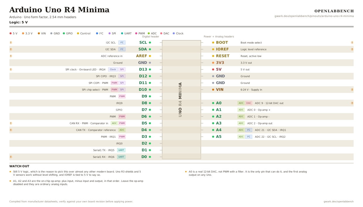
Fig. 1. Arduino Uno R4 Minima, Uno form factor, 2.54 mm headers. Hover or tap a signal to light up every pin that carries it.
2.Watch out
- Still 5 V logic, which is the reason to pick this over almost any other modern board. Uno R3 shields and 5 V sensors work without level shifting, and IOREF is tied to 5 V to say so.
- A0 is a real 12-bit DAC, not PWM with a filter. It is the only pin that can do it, and the first analog output on any Uno.
- A1, A2 and A3 are the on-chip op-amp: plus input, minus input and output, in that order. Leave the op-amp disabled and they are ordinary analog inputs.
- CAN is on D4 and D5, and the official datasheet gets this backwards in its description column. The pinout diagram's peripheral table is right: D4 is CTX0, the transmitter, and D5 is CRX0, the receiver. Either way you still need an external transceiver; these are logic-level pins.
- Not every pin can raise an interrupt. The RA4M1 routes IRQ lines to D0, D1, D2, D3, D8, D12, D13, A4 and A5 only, which is a trap if you are porting code from a board where every pin could.
- PWM is on D3, D5, D6, D9, D10 and D11. D13 cannot do it any more, which breaks a surprising amount of old Uno example code.
- A4 and A5 are the same silicon pins as D18 and D19, and they carry I2C. You get the analog input or the I2C bus, not both at once.
- The ADC will do 14 bits if you ask for it with analogReadResolution. It defaults to 10 for compatibility with code written for the R3.
- Position 1 on the power header is BOOT on this board, where the R3 had an unconnected pin. The barrel jack takes 6 to 24 V, a much wider range than the R3 was happy with.
3.Full pin reference
Every pin, alias and mapping. This is the table that prints.
Table 1. Pin assignments.
| Pin | Name | Also called | Functions | Notes |
|---|---|---|---|---|
| - | SCLI²C | D19, A5, P100 | I2C SCL | Same silicon pin as A5, duplicated on the header for shields. |
| - | SDAI²C | D18, A4, P101 | I2C SDA | Same silicon pin as A4. |
| - | AREF | - | ADC reference in | Only drive this after switching the reference in software. |
| - | GND | - | Ground | |
| - | D13SPIClock | SCK, P111 | SPI clock, On-board LED, IRQ4 | The LED pin, and no longer PWM capable. |
| - | D12SPI | CIPO, MISO, P110 | SPI CIPO, IRQ3 | |
| - | D11SPIPWM | COPI, MOSI, P109 | SPI COPI, PWM | |
| - | D10SPIPWM | CS, SS, P112 | SPI chip select, PWM | |
| - | D9PWM | P303 | PWM | |
| - | D8 | P304 | IRQ9 | |
| - | D7 | P107 | GPIO | |
| - | D6PWM | P106 | PWM | |
| - | D5PWMADC | CANRX0, P102 | CAN RX, PWM, Comparator in | CAN receive, despite what the datasheet's description column says. |
| - | D4ADC | CANTX0, P103 | CAN TX, Comparator reference | CAN transmit. Needs an external transceiver to reach a bus. |
| - | D3PWM | P104 | PWM, IRQ1 | |
| - | D2 | P105 | IRQ0 | |
| - | D1UART | TX, TX0, P302 | Serial1 TX, IRQ5 | |
| - | D0UART | RX, RX0, P301 | Serial1 RX, IRQ6 | Receive, not transmit. The datasheet's pin table misprints this one as TX0. |
| - | BOOT | - | Boot mode select | Where the R3 had an unconnected pin. It picks the boot mode at reset. |
| - | IOREF | - | Logic level reference | Tied to 5 V. A shield reads this to find out what levels the board speaks. |
| - | RESET | - | Reset, active low | |
| - | 3V3 | - | 3.3 V out | |
| - | 5V | - | 5 V out | |
| - | GND | - | Ground | |
| - | GND | - | Ground | |
| - | VIN6-24 V | - | Supply in | Shared with the barrel jack, through a buck converter rather than a linear regulator. |
| - | A0ADCDAC | D14, P014, DAC | ADC 9, 12-bit DAC out | The only true analog output on the board. |
| - | A1ADC | D15, P000 | ADC 0, Op-amp + | |
| - | A2ADC | D16, P001 | ADC 1, Op-amp - | |
| - | A3ADC | D17, P002 | ADC 2, Op-amp out | |
| - | A4ADCI²C | D18, SDA, P101 | ADC 21, I2C SDA, IRQ1 | |
| - | A5ADCI²C | D19, SCL, P100 | ADC 22, I2C SCL, IRQ2 |
Found a wrong pin? The whole board is one file, data/boards/arduino-uno-r4-minima.json.