Atmel / Microchip · Microcontroller
AT89S52 (8051)
The 8051 that is still buyable and still in every embedded syllabus. Four 8-bit ports, in-system programmable, DIP-40.
- Logic level
- 4.0-5.5 V
- Package
- PDIP-40 / PLCC-44 / TQFP-44
1.Pinout diagram
Highlight a signalhover to preview, click to keep
Pins 1-20
Pins 21-40
Pin detail
Hover a pin for its mappings and gotchas. Click to keep it here.
- Logic level
- 4.0-5.5 V
- Package
- PDIP-40 / PLCC-44 / TQFP-44
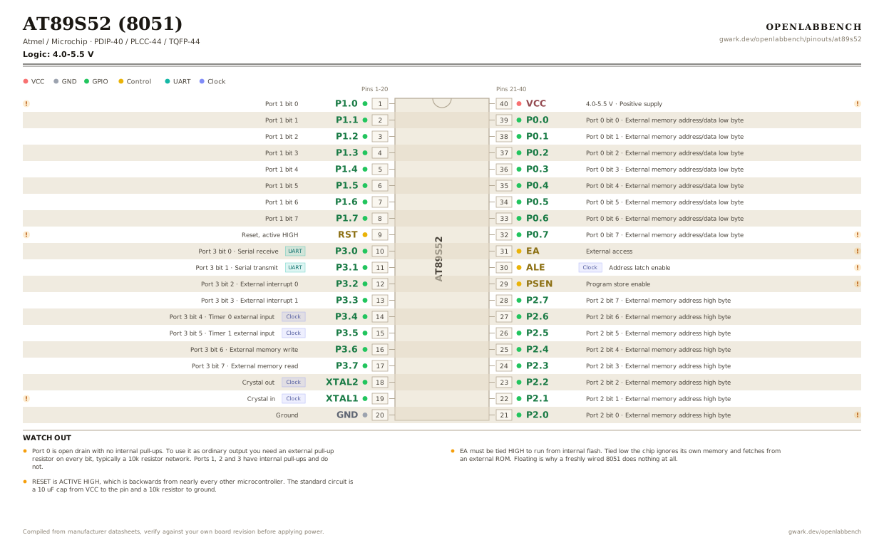
Fig. 1. AT89S52 (8051), PDIP-40. Hover or tap a signal to light up every pin that carries it.
2.Watch out
- Port 0 is open drain with no internal pull-ups. To use it as ordinary output you need an external pull-up resistor on every bit, typically a 10k resistor network. Ports 1, 2 and 3 have internal pull-ups and do not.
- EA must be tied HIGH to run from internal flash. Tied low the chip ignores its own memory and fetches from an external ROM. Floating is why a freshly wired 8051 does nothing at all.
- RESET is ACTIVE HIGH, which is backwards from nearly every other microcontroller. The standard circuit is a 10 uF cap from VCC to the pin and a 10k resistor to ground.
- 11.0592 MHz is the traditional crystal because it divides exactly into 9600 and the other standard baud rates. 12 MHz gives round instruction timings but ugly baud rates.
- The classic 8051 takes 12 clock cycles per machine cycle, so an 11.0592 MHz part runs under a million instructions a second. Single-cycle cores like the STC and the Silicon Labs C8051 are an order of magnitude faster at the same crystal.
- The S in AT89S52 means in-system programmable over SPI, using MOSI, MISO and SCK on P1.5, P1.6 and P1.7. The older AT89C52 needs a parallel programmer.
- Ports 0 and 2 become the address and data bus if you attach external memory, which leaves you Port 1 and Port 3 for everything else.
3.Minimum circuit to run
What has to go around the chip before it will run.
| Part | Between | Why |
|---|---|---|
| Wire link | EA (31) to VCC | EA low makes the chip fetch all code from external memory. Tie it high or the flash is ignored. |
| 10 uF | VCC to RST (9) | Power-on reset. Reset is active high on the 8051, so the capacitor pulls RST up at power-up. |
| 10 kOhm | RST (9) to GND | Discharges the reset capacitor so RST settles low once the supply is stable. |
| 11.0592 MHz crystal | XTAL1 (19) to XTAL2 (18) | No internal oscillator. That frequency divides to exact standard baud rates, which is why it is everywhere. |
| 30 pF | XTAL1 (19) to GND | Crystal load capacitor. |
| 30 pF | XTAL2 (18) to GND | The matching load capacitor. |
| 100 nF | VCC (40) to GND | Supply decoupling at the pin. |
| 10 kOhmoptional | P0.0 (39) to VCC | Port 0 is open drain with no internal pull-ups. One resistor to VCC per P0 line you actually use. |
Reset is active high here, the opposite of almost every other micro on this site. Holding RST high holds the chip in reset.
4.Register configuration
Turning a pin on the diagram into a configured pin.
Use the quasi-bidirectional ports
SDCC or Keil C51
#include <reg52.h>

/* There is no direction register. Write 1 to a bit to release it
   so it can be read, write 0 to pull it low. */

P2 = 0x00;                     /* drive all of Port 2 low  */
P2 = 0xFF;                     /* release it, weakly high  */

P1 = 0xFF;                     /* release Port 1 to read it */
if ((P1 & 0x01) == 0) {        /* P1.0 pulled to ground     */
}

sbit LED = P2 ^ 0;             /* single bit access */
LED = 0;
Port 0 has no internal pull-ups at all, so it cannot drive a logic high without an external resistor on every bit. Ports 1, 2 and 3 have weak ones and can.
5.Full pin reference
Every pin, alias and mapping. This is the table that prints.
Table 2. Pin assignments.
| Pin | Name | Also called | Functions | Notes |
|---|---|---|---|---|
| 1 | P1.0 | - | Port 1 bit 0 | Port 1 has internal pull-ups and is the only port that is plain I/O with no second job. |
| 2 | P1.1 | - | Port 1 bit 1 | |
| 3 | P1.2 | - | Port 1 bit 2 | |
| 4 | P1.3 | - | Port 1 bit 3 | |
| 5 | P1.4 | - | Port 1 bit 4 | |
| 6 | P1.5 | - | Port 1 bit 5 | |
| 7 | P1.6 | - | Port 1 bit 6 | |
| 8 | P1.7 | - | Port 1 bit 7 | |
| 9 | RST | - | Reset, active HIGH | Active high, unlike almost every other microcontroller. Hold high for two machine cycles. A cap to VCC and a resistor to ground is the standard power-on circuit. |
| 10 | P3.0UART | RXD | Port 3 bit 0, Serial receive | |
| 11 | P3.1UART | TXD | Port 3 bit 1, Serial transmit | |
| 12 | P3.2 | INT0 | Port 3 bit 2, External interrupt 0 | |
| 13 | P3.3 | INT1 | Port 3 bit 3, External interrupt 1 | |
| 14 | P3.4Clock | T0 | Port 3 bit 4, Timer 0 external input | |
| 15 | P3.5Clock | T1 | Port 3 bit 5, Timer 1 external input | |
| 16 | P3.6 | WR | Port 3 bit 6, External memory write | |
| 17 | P3.7 | RD | Port 3 bit 7, External memory read | |
| 18 | XTAL2Clock | - | Crystal out | |
| 19 | XTAL1Clock | - | Crystal in | 11.0592 MHz is the traditional choice because it divides exactly into standard baud rates. |
| 20 | GND | VSS | Ground | |
| 21 | P2.0 | - | Port 2 bit 0, External memory address high byte | Port 2 carries A8 to A15 when external memory is in use. |
| 22 | P2.1 | - | Port 2 bit 1, External memory address high byte | |
| 23 | P2.2 | - | Port 2 bit 2, External memory address high byte | |
| 24 | P2.3 | - | Port 2 bit 3, External memory address high byte | |
| 25 | P2.4 | - | Port 2 bit 4, External memory address high byte | |
| 26 | P2.5 | - | Port 2 bit 5, External memory address high byte | |
| 27 | P2.6 | - | Port 2 bit 6, External memory address high byte | |
| 28 | P2.7 | - | Port 2 bit 7, External memory address high byte | |
| 29 | PSEN | /PSEN | Program store enable | Strobe for reading external program memory. Leave open when running from internal flash. |
| 30 | ALEClock | ALE/PROG | Address latch enable | Pulses at one sixth of the crystal frequency, which makes a handy clock source if you need one. |
| 31 | EA | /EA, VPP | External access | Tie HIGH to run from internal flash. Tie low and the chip ignores its own memory entirely and fetches from an external ROM. Leaving it floating is why a fresh 8051 does nothing. |
| 32 | P0.7 | - | Port 0 bit 7, External memory address/data low byte | Port 0 is open drain with NO internal pull-ups. It needs external pull-ups to work as ordinary output, which catches everyone once. |
| 33 | P0.6 | - | Port 0 bit 6, External memory address/data low byte | |
| 34 | P0.5 | - | Port 0 bit 5, External memory address/data low byte | |
| 35 | P0.4 | - | Port 0 bit 4, External memory address/data low byte | |
| 36 | P0.3 | - | Port 0 bit 3, External memory address/data low byte | |
| 37 | P0.2 | - | Port 0 bit 2, External memory address/data low byte | |
| 38 | P0.1 | - | Port 0 bit 1, External memory address/data low byte | |
| 39 | P0.0 | - | Port 0 bit 0, External memory address/data low byte | |
| 40 | VCC4.0-5.5 V | - | Positive supply | 100 nF at the pin. |
Primary sources
Found a wrong pin? The whole board is one file, data/boards/at89s52.json.