Microchip (Atmel) · Microcontroller
ATmega328P (PDIP-28)
The chip inside the Uno and Nano, on its own in a 28-pin DIP. Useful when you want the Arduino toolchain on a bare board. The mapping between port pins and Arduino numbers is the part nobody remembers.
- Logic level
- 1.8-5.5 V
- Package
- PDIP-28 / TQFP-32 / MLF-32
1.Pinout diagram
Highlight a signalhover to preview, click to keep
Pins 1-14
Pins 15-28
Pin detail
Hover a pin for its mappings and gotchas. Click to keep it here.
- Logic level
- 1.8-5.5 V
- Package
- PDIP-28 / TQFP-32 / MLF-32
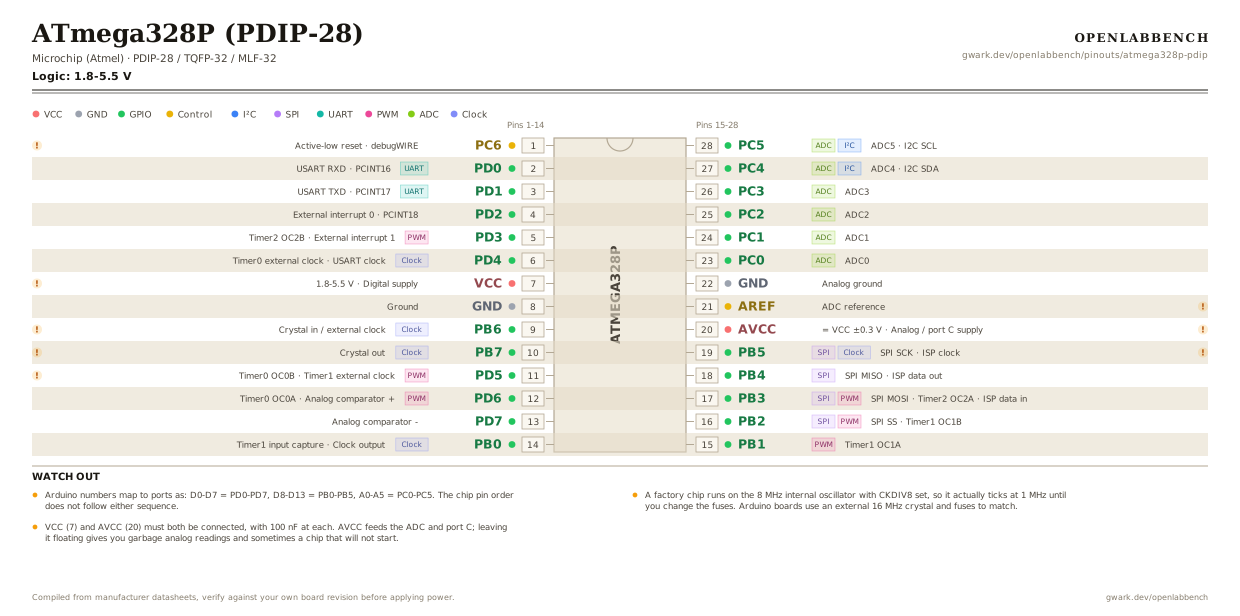
Fig. 1. ATmega328P (PDIP-28), PDIP-28. Hover or tap a signal to light up every pin that carries it.
2.Watch out
- Arduino numbers map to ports as: D0-D7 = PD0-PD7, D8-D13 = PB0-PB5, A0-A5 = PC0-PC5. The chip pin order does not follow either sequence.
- A factory chip runs on the 8 MHz internal oscillator with CKDIV8 set, so it actually ticks at 1 MHz until you change the fuses. Arduino boards use an external 16 MHz crystal and fuses to match.
- VCC (7) and AVCC (20) must both be connected, with 100 nF at each. AVCC feeds the ADC and port C; leaving it floating gives you garbage analog readings and sometimes a chip that will not start.
- PB6/PB7 (9/10) are the crystal pins. On the internal oscillator they free up as two extra I/O, but the Arduino core does not expose them.
- RESET (1) needs a 10k pull-up to VCC. It is also the dW debug pin, and disabling it via fuse locks out ISP programming.
- 20 mA per pin recommended, 40 mA absolute max, 200 mA total through VCC/GND.
- The ATmega328PB is a newer die with extra peripherals, but it is not a silent drop-in: some register names and vector numbers changed.
- The speed grade tracks the supply: 20 MHz needs at least 4.5 V, 10 MHz needs 2.7 V, and 4 MHz works down to 1.8 V. Running a 16 MHz crystal on 3.3 V is out of spec, which is why 3.3 V Pro Minis ship at 8 MHz.
3.Minimum circuit to run
What has to go around the chip before it will run.
| Part | Between | Why |
|---|---|---|
| 100 nF | VCC (7) to GND | Supply decoupling, as close to the pins as the layout allows. |
| 100 nF | AVCC (20) to GND | The analog supply needs its own decoupling even if you never use the ADC. |
| Wire link | AVCC (20) to VCC | AVCC must be powered or the ADC and all of port C misbehave. |
| 10 kOhm | PC6 (1) to VCC | There is no internal pull-up strong enough. A floating RESET gives random restarts. |
| 16 MHz crystaloptional | PB6 (9) to PB7 (10) | Only if you want 16 MHz. The internal 8 MHz RC needs no parts at all. |
| 22 pFoptional | PB6 (9) to GND | Crystal load capacitor. Omit it and the oscillator may not start. |
| 22 pFoptional | PB7 (10) to GND | The other crystal load capacitor. |
| 100 nFoptional | AREF (21) to GND | Quietens the ADC reference. |
A factory chip runs on the internal 8 MHz RC with CKDIV8 set, so it ticks at 1 MHz until you change the fuses. Fitting the crystal is not enough on its own; the fuses have to select it.
4.Register configuration
Turning a pin on the diagram into a configured pin.
Drive a pin, and read one with a pull-up
avr-libc
#include <avr/io.h>

/* Three registers per port. DDR picks direction, PORT writes the
   output latch, PIN reads the physical pin. */

DDRB  |=  (1 << PB5);          /* PB5 = Arduino D13 = output */
PORTB |=  (1 << PB5);          /* high */
PORTB &= ~(1 << PB5);          /* low  */
PINB  |=  (1 << PB5);          /* writing PIN toggles the output */

DDRD  &= ~(1 << PD2);          /* PD2 = D2 = input */
PORTD |=  (1 << PD2);          /* PORT on an input enables the pull-up */

if (!(PIND & (1 << PD2))) {    /* switch to ground reads 0 when pressed */
}
On an input pin, PORT is the pull-up enable, not an output value. Forget it and a floating pin reads whatever the nearest mains cable is doing.
5.Full pin reference
Every pin, alias and mapping. This is the table that prints.
Table 2. Pin assignments.
| Pin | Name | Also called | Functions | Notes |
|---|---|---|---|---|
| 1 | PC6 | RESET, dW | Active-low reset, debugWIRE | 10k pull-up to VCC required. |
| 2 | PD0UART | D0, RXD | USART RXD, PCINT16 | |
| 3 | PD1UART | D1, TXD | USART TXD, PCINT17 | |
| 4 | PD2 | D2, INT0 | External interrupt 0, PCINT18 | |
| 5 | PD3PWM | D3, INT1, OC2B | Timer2 OC2B, External interrupt 1 | |
| 6 | PD4Clock | D4, T0, XCK | Timer0 external clock, USART clock | |
| 7 | VCC1.8-5.5 V | - | Digital supply | 100 nF at the pin. |
| 8 | GND | - | Ground | |
| 9 | PB6Clock | XTAL1, TOSC1 | Crystal in / external clock | Free as I/O only on the internal oscillator. |
| 10 | PB7Clock | XTAL2, TOSC2 | Crystal out | Free as I/O only on the internal oscillator. |
| 11 | PD5PWM | D5, T1, OC0B | Timer0 OC0B, Timer1 external clock | Timer0 also drives millis(), do not reprogram its prescaler. |
| 12 | PD6PWM | D6, AIN0, OC0A | Timer0 OC0A, Analog comparator + | |
| 13 | PD7 | D7, AIN1 | Analog comparator - | |
| 14 | PB0Clock | D8, ICP1, CLKO | Timer1 input capture, Clock output | |
| 15 | PB1PWM | D9, OC1A | Timer1 OC1A | |
| 16 | PB2SPIPWM | D10, SS, OC1B | SPI SS, Timer1 OC1B | |
| 17 | PB3SPIPWM | D11, MOSI, OC2A | SPI MOSI, Timer2 OC2A, ISP data in | |
| 18 | PB4SPI | D12, MISO | SPI MISO, ISP data out | |
| 19 | PB5SPIClock | D13, SCK | SPI SCK, ISP clock | The on-board LED pin on Arduino boards. |
| 20 | AVCC= VCC ±0.3 V | - | Analog / port C supply | Must be connected even if the ADC is unused. 100 nF, or an LC filter from VCC for quiet readings. |
| 21 | AREF | - | ADC reference | 100 nF to ground. Only drive it externally after selecting the external reference. |
| 22 | GND | - | Analog ground | |
| 23 | PC0ADC | A0, ADC0 | ADC0 | |
| 24 | PC1ADC | A1, ADC1 | ADC1 | |
| 25 | PC2ADC | A2, ADC2 | ADC2 | |
| 26 | PC3ADC | A3, ADC3 | ADC3 | |
| 27 | PC4ADCI²C | A4, ADC4, SDA | ADC4, I2C SDA | |
| 28 | PC5ADCI²C | A5, ADC5, SCL | ADC5, I2C SCL |
Looking for a substitute?
Primary sources
Found a wrong pin? The whole board is one file, data/boards/atmega328p-pdip.json.