Microchip (Atmel) · Microcontroller
ATtiny85 (PDIP-8)
8 KB AVR in an 8-pin package with five usable I/O. Every pin does three or four jobs, so the whole design problem is deciding what each one gives up.
- Logic level
- 1.8-5.5 V
- Package
- PDIP-8 / SOIC-8 / TSSOP-8 / QFN-20
1.Pinout diagram
Highlight a signalhover to preview, click to keep
Pins 1-4
Pins 5-8
Pin detail
Hover a pin for its mappings and gotchas. Click to keep it here.
- Logic level
- 1.8-5.5 V
- Package
- PDIP-8 / SOIC-8 / TSSOP-8 / QFN-20
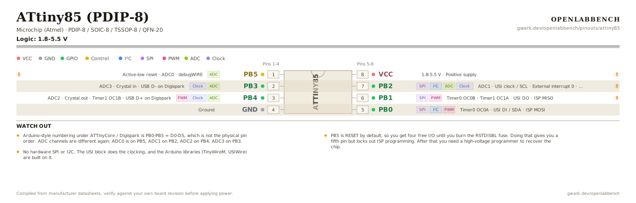
Fig. 1. ATtiny85 (PDIP-8), PDIP-8. Hover or tap a signal to light up every pin that carries it.
2.Watch out
- Arduino-style numbering under ATTinyCore / Digispark is PB0-PB5 = D0-D5, which is not the physical pin order. ADC channels are different again: ADC0 is on PB5, ADC1 on PB2, ADC2 on PB4, ADC3 on PB3.
- PB5 is RESET by default, so you get four free I/O until you burn the RSTDISBL fuse. Doing that gives you a fifth pin but locks out ISP programming. After that you need a high-voltage programmer to recover the chip.
- No hardware SPI or I2C. The USI block does the clocking, and the Arduino libraries (TinyWireM, USIWire) are built on it.
- There is no hardware UART. Serial on an ATtiny85 is bit-banged software serial.
- The USB bootloader boards (Digispark, micronucleus) take PB3 and PB4 for D- and D+, leaving PB0, PB1 and PB2.
- Default fuses give 8 MHz internal with CKDIV8, so a fresh chip runs at 1 MHz. 16.5 MHz from the internal PLL is available and is what USB bootloaders use.
- The speed grade tracks the supply, as on the ATmega328P: 20 MHz needs 4.5 V, 10 MHz needs 2.7 V.
3.Minimum circuit to run
What has to go around the chip before it will run.
| Part | Between | Why |
|---|---|---|
| 100 nF | VCC (8) to GND | Supply decoupling at the pin. |
| 10 kOhm | PB5 (1) to VCC | Needed unless you have burned the RSTDISBL fuse, which is a one-way trip without a high-voltage programmer. |
No crystal needed. The internal oscillator covers 1, 8 and 16.5 MHz, and the USB bootloader boards rely on it.
4.Register configuration
Turning a pin on the diagram into a configured pin.
Drive a pin on the only port there is
avr-libc
#include <avr/io.h>

/* Everything lives on port B. PB0 to PB4 are free; PB5 is RESET
   until you burn a fuse you cannot easily undo. */

DDRB  |=  (1 << PB1);          /* PB1 = pin 6, the LED on most boards */
PORTB |=  (1 << PB1);
PORTB &= ~(1 << PB1);

DDRB  &= ~(1 << PB2);          /* PB2 = pin 7, input */
PORTB |=  (1 << PB2);          /* internal pull-up */

if (!(PINB & (1 << PB2))) {
}
Arduino numbering under ATTinyCore is PB0 to PB5 = D0 to D5, which is not the physical pin order. PB1 is physical pin 6.
5.Full pin reference
Every pin, alias and mapping. This is the table that prints.
Table 2. Pin assignments.
| Pin | Name | Also called | Functions | Notes |
|---|---|---|---|---|
| 1 | PB5ADC | RESET, D5, A0, ADC0, dW | Active-low reset, ADC0, debugWIRE | Reset by default; needs a 10k pull-up. Usable as I/O only after disabling reset by fuse. |
| 2 | PB3ADCClock | D3, A3, ADC3, XTAL1, CLKI | ADC3, Crystal in, USB D- on Digispark | |
| 3 | PB4ADCClockPWM | D4, A2, ADC2, XTAL2, CLKO | ADC2, Crystal out, Timer1 OC1B, USB D+ on Digispark | |
| 4 | GND | - | Ground | |
| 5 | PB0SPII²CPWM | D0, MOSI, DI, SDA, AIN0, OC0A | Timer0 OC0A, USI DI / SDA, ISP MOSI | |
| 6 | PB1SPIPWM | D1, MISO, DO, AIN1, OC0B, OC1A | Timer0 OC0B, Timer1 OC1A, USI DO, ISP MISO | The LED pin on most ATtiny85 dev boards. |
| 7 | PB2SPII²CADCClock | D2, SCK, USCK, SCL, A1, ADC1, INT0, T0 | ADC1, USI clock / SCL, External interrupt 0, ISP SCK | The only pin with a true external interrupt. |
| 8 | VCC1.8-5.5 V | - | Positive supply | 100 nF at the pin. |
Looking for a substitute?
Primary sources
Found a wrong pin? The whole board is one file, data/boards/attiny85.json.