BeagleBoard.org · Single-board computer
BeagleBone Black P9 Header
The power, serial, I2C, SPI and analog side of the BeagleBone Black. The seven ADC channels take 1.8 V at most.
- Logic level
- 3.3 V / 1.8 V ADC
- Package
- 2x23 2.54 mm (P9)
1.Pinout diagram
Highlight a signalhover to preview, click to keep
Odd pins
BBB P9
Even pins
Pin detail
Hover a pin for its mappings and gotchas. Click to keep it here.
- Logic level
- 3.3 V / 1.8 V ADC
- Package
- 2x23 2.54 mm (P9)
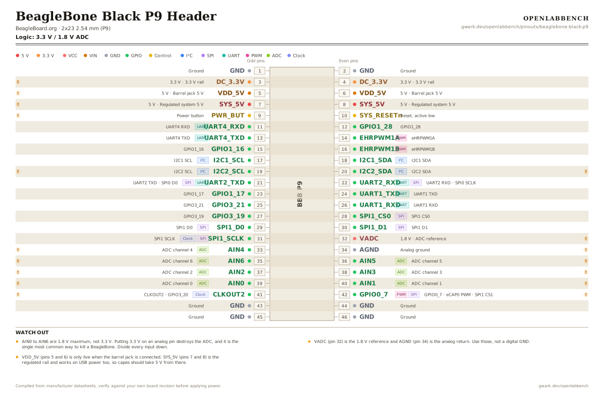
Fig. 1. BeagleBone Black P9 Header, 2x23 2.54 mm (P9). Hover or tap a signal to light up every pin that carries it.
2.Watch out
- AIN0 to AIN6 are 1.8 V maximum, not 3.3 V. Putting 3.3 V on an analog pin destroys the ADC, and it is the single most common way to kill a BeagleBone. Divide every input down.
- VADC (pin 32) is the 1.8 V reference and AGND (pin 34) is the analog return. Use those, not a digital GND.
- VDD_5V (pins 5 and 6) is only live when the barrel jack is connected. SYS_5V (pins 7 and 8) is the regulated rail and works on USB power too, so capes should take 5 V from there.
- I2C2 on pins 19 and 20 is the cape EEPROM bus and already has pull-ups. You can hang other devices on it, but address 0x54 to 0x57 are reserved for cape EEPROMs.
- Pins 41 and 42 are each wired to two processor balls. Whichever one you are not using must be set to input, or the two fight each other.
- Signal names here are the power-on defaults. Almost every pin can be muxed to something else through the device tree, which is both the strength and the learning curve of this board.
- GPIO are 3.3 V and not 5 V tolerant. Source or sink 4 to 6 mA per pin, far less than a Pi.
- The other side of this board is the P8 header, documented separately: gwark.dev/openlabbench/pinouts/beaglebone-black-p8
3.Full pin reference
Every pin, alias and mapping. This is the table that prints.
Table 1. Pin assignments.
| Pin | Name | Also called | Functions | Notes |
|---|---|---|---|---|
| 1 | GND | - | Ground | |
| 2 | GND | - | Ground | |
| 3 | DC_3.3V3.3 V | - | 3.3 V rail | 250 mA budget across both 3.3 V pins. |
| 4 | DC_3.3V3.3 V | - | 3.3 V rail | |
| 5 | VDD_5V5 V | - | Barrel jack 5 V | Only live when the barrel jack is plugged in, not on USB power. 1 A for capes. |
| 6 | VDD_5V5 V | - | Barrel jack 5 V | |
| 7 | SYS_5V5 V | - | Regulated system 5 V | Present on USB power too. This is the one to use for a cape. |
| 8 | SYS_5V5 V | - | Regulated system 5 V | |
| 9 | PWR_BUT | - | Power button | Pull low to request a soft shutdown. |
| 10 | SYS_RESETn | A10 | Reset, active low | |
| 11 | UART4_RXDUART | T17, GPIO0_30 | UART4 RXD | |
| 12 | GPIO1_28 | U18 | GPIO1_28 | |
| 13 | UART4_TXDUART | U17, GPIO0_31 | UART4 TXD | |
| 14 | EHRPWM1APWM | U14, GPIO1_18 | eHRPWM1A | |
| 15 | GPIO1_16 | R13 | GPIO1_16 | |
| 16 | EHRPWM1BPWM | T14, GPIO1_19 | eHRPWM1B | |
| 17 | I2C1_SCLI²C | A16, GPIO0_5 | I2C1 SCL | |
| 18 | I2C1_SDAI²C | B16, GPIO0_4 | I2C1 SDA | |
| 19 | I2C2_SCLI²C | D17, GPIO0_13 | I2C2 SCL | I2C2 is the cape EEPROM bus and already has pull-ups fitted. |
| 20 | I2C2_SDAI²C | D18, GPIO0_12 | I2C2 SDA | Cape EEPROM bus, pull-ups already fitted. |
| 21 | UART2_TXDUARTSPI | B17, GPIO0_3 | UART2 TXD, SPI0 D0 | |
| 22 | UART2_RXDUARTSPI | A17, GPIO0_2 | UART2 RXD, SPI0 SCLK | |
| 23 | GPIO1_17 | V14 | GPIO1_17 | |
| 24 | UART1_TXDUART | D15, GPIO0_15 | UART1 TXD | |
| 25 | GPIO3_21 | A14 | GPIO3_21 | |
| 26 | UART1_RXDUART | D16, GPIO0_14 | UART1 RXD | |
| 27 | GPIO3_19 | C13 | GPIO3_19 | |
| 28 | SPI1_CS0SPI | C12, GPIO3_17 | SPI1 CS0 | |
| 29 | SPI1_D0SPI | B13, GPIO3_15 | SPI1 D0 | |
| 30 | SPI1_D1SPI | D12, GPIO3_16 | SPI1 D1 | |
| 31 | SPI1_SCLKSPIClock | A13, GPIO3_14 | SPI1 SCLK | |
| 32 | VADC1.8 V | - | ADC reference | 1.8 V reference for the analog inputs. Not a rail to power things from. |
| 33 | AIN4ADC | C8 | ADC channel 4 | Analog in, 1.8 V MAX. 3.3 V here destroys the ADC. Scale every input. |
| 34 | AGND | - | Analog ground | Return for the ADC. Keep analog returns off the digital GND pins. |
| 35 | AIN6ADC | A8 | ADC channel 6 | Analog in, 1.8 V MAX. 3.3 V here destroys the ADC. Scale every input. |
| 36 | AIN5ADC | B8 | ADC channel 5 | Analog in, 1.8 V MAX. 3.3 V here destroys the ADC. Scale every input. |
| 37 | AIN2ADC | B7 | ADC channel 2 | Analog in, 1.8 V MAX. 3.3 V here destroys the ADC. Scale every input. |
| 38 | AIN3ADC | A7 | ADC channel 3 | Analog in, 1.8 V MAX. 3.3 V here destroys the ADC. Scale every input. |
| 39 | AIN0ADC | B6 | ADC channel 0 | Analog in, 1.8 V MAX. 3.3 V here destroys the ADC. Scale every input. |
| 40 | AIN1ADC | C7 | ADC channel 1 | Analog in, 1.8 V MAX. 3.3 V here destroys the ADC. Scale every input. |
| 41 | CLKOUT2Clock | D14, GPIO3_20, D13 | CLKOUT2, GPIO3_20 | Shared between two processor balls, D14 and D13. Set whichever one you are not using to input. |
| 42 | GPIO0_7PWMSPI | C18, GPIO3_18, B12 | GPIO0_7, eCAP0 PWM, SPI1 CS1 | Shared between two processor balls, C18 and B12. Set the unused one to input. |
| 43 | GND | - | Ground | |
| 44 | GND | - | Ground | |
| 45 | GND | - | Ground | |
| 46 | GND | - | Ground |
Found a wrong pin? The whole board is one file, data/boards/beaglebone-black-p9.json.