TI / ON / many · Integrated circuit
CD4051 8-Channel Analog Mux
One analog pin becomes eight. Bidirectional, so it multiplexes sensors into an ADC or fans a signal back out.
- Logic level
- 3-18 V (CD4051), 2-10 V (74HC4051)
- Package
- PDIP-16 / SOIC-16
1.Pinout diagram
Highlight a signalhover to preview, click to keep
Pins 1-8
Pins 9-16
Pin detail
Hover a pin for its mappings and gotchas. Click to keep it here.
- Logic level
- 3-18 V (CD4051), 2-10 V (74HC4051)
- Package
- PDIP-16 / SOIC-16
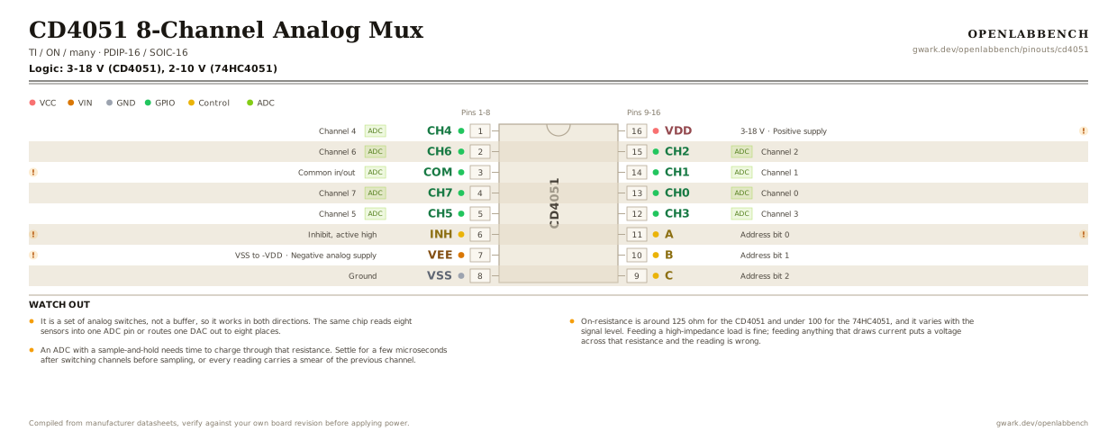
Fig. 1. CD4051 8-Channel Analog Mux, PDIP-16. Hover or tap a signal to light up every pin that carries it.
2.Watch out
- It is a set of analog switches, not a buffer, so it works in both directions. The same chip reads eight sensors into one ADC pin or routes one DAC out to eight places.
- On-resistance is around 125 ohm for the CD4051 and under 100 for the 74HC4051, and it varies with the signal level. Feeding a high-impedance load is fine; feeding anything that draws current puts a voltage across that resistance and the reading is wrong.
- An ADC with a sample-and-hold needs time to charge through that resistance. Settle for a few microseconds after switching channels before sampling, or every reading carries a smear of the previous channel.
- Three address pins select the channel, A is the low bit. INH high disconnects everything, which is how you parallel several chips onto one bus.
- VEE is the negative analog rail. Tie it to ground for single-supply work; tie it to a negative rail and the chip will pass signals that swing below ground, which no microcontroller input can do alone.
- The channel pins are scattered around the package in no sensible order. Wire from the numbers.
- For 16 channels the CD4067 is the same idea with four address pins.
3.Minimum circuit
What has to go around the chip before it will run.
| Part | Between | Why |
|---|---|---|
| Wire link | VEE (7) to GND | VEE sets the bottom of the analog range. On a single supply it goes to ground, and it must go somewhere. |
| Wire link | INH (6) to GND | Inhibit is active high. Held high, all eight channels stay disconnected. |
| 100 nF | VDD (16) to GND | Supply decoupling at the pin. |
VDD sets the largest signal the switches will pass, and the three address pins are digital inputs that must be driven, never left floating. With VEE on a negative rail the part switches signals that swing below ground, which is the reason to choose a 4051 over a 74HC4051.
4.Full pin reference
Every pin, alias and mapping. This is the table that prints.
Table 2. Pin assignments.
| Pin | Name | Also called | Functions | Notes |
|---|---|---|---|---|
| 1 | CH4ADC | - | Channel 4 | |
| 2 | CH6ADC | - | Channel 6 | |
| 3 | COMADC | Z, COMMON | Common in/out | The single pin that connects to whichever channel is selected. |
| 4 | CH7ADC | - | Channel 7 | |
| 5 | CH5ADC | - | Channel 5 | |
| 6 | INH | E, ENABLE | Inhibit, active high | Ground it to enable. High disconnects all eight channels. |
| 7 | VEEVSS to -VDD | - | Negative analog supply | Tie to ground for single supply. A negative rail here lets signals swing below ground. |
| 8 | VSS | GND | Ground | |
| 9 | C | S3, A2 | Address bit 2 | |
| 10 | B | S2, A1 | Address bit 1 | |
| 11 | A | S1, A0 | Address bit 0 | Low bit of the channel number. |
| 12 | CH3ADC | - | Channel 3 | |
| 13 | CH0ADC | - | Channel 0 | |
| 14 | CH1ADC | - | Channel 1 | |
| 15 | CH2ADC | - | Channel 2 | |
| 16 | VDD3-18 V | - | Positive supply | Sets the maximum signal the switches will pass. 100 nF at the pin. |
Looking for a substitute?
Primary sources
Found a wrong pin? The whole board is one file, data/boards/cd4051.json.