WCH · Microcontroller
CH32V003 RISC-V Microcontroller
A 48 MHz RISC-V part that costs about ten cents, runs from 2.7 to 5.5 V and needs one capacitor to start. Programmed over a single wire.
- Logic level
- 2.7-5.5 V
- Package
- TSSOP-20 (F4P6)
1.Pinout diagram
Highlight a signalhover to preview, click to keep
Pins 1-10
Pins 11-20
Pin detail
Hover a pin for its mappings and gotchas. Click to keep it here.
- Logic level
- 2.7-5.5 V
- Package
- TSSOP-20 (F4P6)
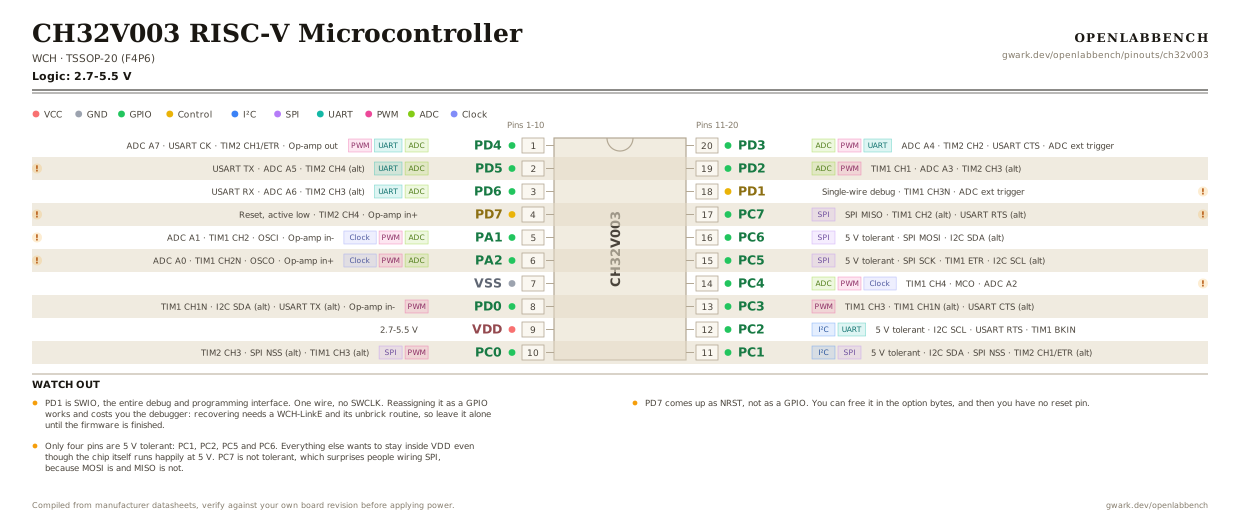
Fig. 1. CH32V003 RISC-V Microcontroller, TSSOP-20 (F4P6). Hover or tap a signal to light up every pin that carries it.
2.Watch out
- PD1 is SWIO, the entire debug and programming interface. One wire, no SWCLK. Reassigning it as a GPIO works and costs you the debugger: recovering needs a WCH-LinkE and its unbrick routine, so leave it alone until the firmware is finished.
- PD7 comes up as NRST, not as a GPIO. You can free it in the option bytes, and then you have no reset pin.
- Only four pins are 5 V tolerant: PC1, PC2, PC5 and PC6. Everything else wants to stay inside VDD even though the chip itself runs happily at 5 V. PC7 is not tolerant, which surprises people wiring SPI, because MOSI is and MISO is not.
- PA1 and PA2 double as OSCI and OSCO for an external 24 MHz crystal. The internal RC oscillator is good enough for almost everything, including USART, so most designs keep both as GPIO.
- 16 KB of flash and 2 KB of SRAM, with the whole 18-pin I/O set on three partial ports: PA has two pins, PC has eight, PD has eight.
- The core is RV32EC: sixteen registers rather than thirty-two, and no hardware multiply or divide on this part. Code built for a full RV32I target will not run.
- A0 through A7 are ADC channels, not port numbers, and they do not line up with the port pin numbers. A0 is on PA2 and A1 is on PA1, which reads backwards the first time.
3.Minimum circuit to run
What has to go around the chip before it will run.
| Part | Between | Why |
|---|---|---|
| 0.1 uF ceramic | VDD (9) to GND | The whole of WCH's reference power supply circuit. One capacitor across VDD and VSS, close to the pins. |
| 0.1 uF ceramicoptional | PD7 (4) to GND | On NRST, for noise immunity. The pull-up is internal, so this is the only external part the reset pin ever needs. |
There is no crystal here and no reset resistor. The oscillator is internal, the reset pull-up is internal, and programming is one wire to PD1. This is close to the smallest part count any 32-bit MCU asks for.
4.Full pin reference
Every pin, alias and mapping. This is the table that prints.
Table 2. Pin assignments.
| Pin | Name | Also called | Functions | Notes |
|---|---|---|---|---|
| 1 | PD4ADCUARTPWM | - | ADC A7, USART CK, TIM2 CH1/ETR, Op-amp out | |
| 2 | PD5ADCUART | - | USART TX, ADC A5, TIM2 CH4 (alt) | Default USART TX, so this is the pin a serial bootloader or printf lands on. |
| 3 | PD6ADCUART | - | USART RX, ADC A6, TIM2 CH3 (alt) | |
| 4 | PD7 | NRST | Reset, active low, TIM2 CH4, Op-amp in+ | Reset after power-up. Becomes a GPIO only if you change the option bytes, and then nothing resets the chip but power. |
| 5 | PA1ADCPWMClock | - | ADC A1, TIM1 CH2, OSCI, Op-amp in- | Crystal input if you fit one. ADC channel 1, not 0. |
| 6 | PA2ADCPWMClock | - | ADC A0, TIM1 CH2N, OSCO, Op-amp in+ | Crystal output if you fit one. ADC channel 0. |
| 7 | VSS | GND | - | |
| 8 | PD0PWM | - | TIM1 CH1N, I2C SDA (alt), USART TX (alt), Op-amp in- | |
| 9 | VDD2.7-5.5 V | - | - | |
| 10 | PC0PWMSPI | - | TIM2 CH3, SPI NSS (alt), TIM1 CH3 (alt) | |
| 11 | PC15 V tolerantI²CSPI | - | I2C SDA, SPI NSS, TIM2 CH1/ETR (alt) | |
| 12 | PC25 V tolerantI²CUART | - | I2C SCL, USART RTS, TIM1 BKIN | |
| 13 | PC3PWM | - | TIM1 CH3, TIM1 CH1N (alt), USART CTS (alt) | |
| 14 | PC4ADCPWMClock | - | TIM1 CH4, MCO, ADC A2 | MCO can output the system clock, which is the easy way to prove the PLL is doing what you think. |
| 15 | PC55 V tolerantSPI | - | SPI SCK, TIM1 ETR, I2C SCL (alt) | |
| 16 | PC65 V tolerantSPI | - | SPI MOSI, I2C SDA (alt) | |
| 17 | PC7SPI | - | SPI MISO, TIM1 CH2 (alt), USART RTS (alt) | Not 5 V tolerant, unlike the other three SPI pins. |
| 18 | PD1 | SWIO | Single-wire debug, TIM1 CH3N, ADC ext trigger | The programming pin. Keep a header on it. |
| 19 | PD2ADCPWM | - | TIM1 CH1, ADC A3, TIM2 CH3 (alt) | |
| 20 | PD3ADCPWMUART | - | ADC A4, TIM2 CH2, USART CTS, ADC ext trigger |
Found a wrong pin? The whole board is one file, data/boards/ch32v003.json.