Ai-Thinker · Dev board
ESP32-CAM (AI-Thinker)
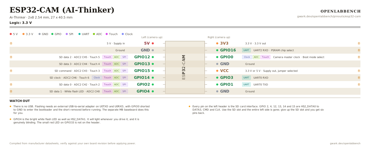
ESP32 with an OV2640 camera and a microSD slot for the price of a sandwich. Almost every exposed pin is already spoken for, and there is no USB. Orientation below has the camera facing up.
- Logic level
- 3.3 V
- Package
- 2x8 2.54 mm, 27 x 40.5 mm
1.Pinout diagram
Highlight a signalhover to preview, click to keep
Left (camera up)
Right (camera up)
Pin detail
Hover a pin for its mappings and gotchas. Click to keep it here.
- Logic level
- 3.3 V
- Package
- 2x8 2.54 mm, 27 x 40.5 mm
Fig. 1. ESP32-CAM (AI-Thinker), 2x8 2.54 mm, 27 x 40.5 mm. Hover or tap a signal to light up every pin that carries it.
2.Watch out
- There is no USB. Flashing needs an external USB-to-serial adapter on U0TXD and U0RXD, with GPIO0 shorted to GND to enter the bootloader and the short removed before running. The separate MB baseboard does this for you.
- Every pin on the left header is the SD card interface. GPIO 2, 4, 12, 13, 14 and 15 are HS2_DATA0 to DATA3, CMD and CLK. Use the SD slot and the entire left side is gone; give up the SD slot and you get six pins back.
- GPIO4 is the bright white flash LED as well as HS2_DATA1. It will light whenever you drive it, and it is genuinely blinding. The small red LED on GPIO33 is not on the header.
- GPIO12 is a strapping pin that must be LOW at boot. It is also an SD data line, which is why a card inserted at power-up sometimes stops the board starting.
- Power it from 5 V, not 3.3 V. The camera plus WiFi pulls bursts well over 200 mA and the on-board regulator needs the headroom. Brownout resets during the first camera init are nearly always an undersized supply or a thin USB cable.
- The pin marked 3.3V/5V is an output, selectable by a solder jumper on the back. It is not a second input.
- GPIO16 is connected to the PSRAM on boards that have it, so treat it as unavailable rather than free.
- Realistically free pins after the camera and SD are accounted for: GPIO 1, 3 and 16 if you give up serial and PSRAM, or GPIO 2, 4, 12, 13, 14 and 15 if you give up the SD card. Plan the project around that, not around sixteen holes.
3.Register configuration
Turning a pin on the diagram into a configured pin.
Drive a pin and read one
ESP-IDF v5
#include "driver/gpio.h"

gpio_reset_pin(GPIO_NUM_2);    /* clears any leftover mux setting */
gpio_set_direction(GPIO_NUM_2, GPIO_MODE_OUTPUT);
gpio_set_level(GPIO_NUM_2, 1);

gpio_config_t in = {
    .pin_bit_mask = 1ULL << GPIO_NUM_4,
    .mode         = GPIO_MODE_INPUT,
    .pull_up_en   = GPIO_PULLUP_ENABLE,
    .intr_type    = GPIO_INTR_NEGEDGE,
};
gpio_config(&in);
pin_bit_mask is 64-bit. Writing 1 << GPIO_NUM_34 instead of 1ULL << overflows a 32-bit int and silently configures nothing.
4.Full pin reference
Every pin, alias and mapping. This is the table that prints.
Table 1. Pin assignments.
| Pin | Name | Also called | Functions | Notes |
|---|---|---|---|---|
| - | 5V5 V | - | Supply in | The pin to power the board from. 3.3 V input browns out during camera init. |
| - | GND | - | Ground | |
| - | GPIO12SPIADCTouch | HS2_DATA2, MTDI | SD data 2, ADC2 CH5, Touch 5 | Strapping pin, must be LOW at boot, and an SD data line. A card inserted at power-up can stop the board starting. |
| - | GPIO13SPIADCTouch | HS2_DATA3, MTCK | SD data 3, ADC2 CH4, Touch 4 | |
| - | GPIO15SPIADCTouch | HS2_CMD, MTDO | SD command, ADC2 CH3, Touch 3 | Strapping pin: high at boot. Pull low to silence the boot log. |
| - | GPIO14SPIADCTouchClock | HS2_CLK, MTMS | SD clock, ADC2 CH6, Touch 6 | |
| - | GPIO2SPIADCTouch | HS2_DATA0 | SD data 0, ADC2 CH2, Touch 2 | Strapping pin: must be low or floating at boot. |
| - | GPIO4SPIADCTouch | HS2_DATA1, FLASH LED | SD data 1, White flash LED, ADC2 CH0 | Drives the bright white LED. It lights whenever you drive this pin, SD card or not. |
| - | 3V33.3 V | - | 3.3 V out | Output from the on-board regulator. |
| - | GPIO16UART | U2RXD | UART2 RXD, PSRAM chip select | Wired to the PSRAM on boards that have it. Treat as unavailable. |
| - | GPIO0ClockADCTouch | CSI_MCLK | Camera master clock, Boot mode select | Short to GND to enter the bootloader, then remove. Also the camera's clock, so it is not a free pin at runtime. |
| - | GND | - | Ground | |
| - | VCC3.3 V or 5 V | - | Supply out, jumper selected | An output, not an input. A solder jumper on the back picks 3.3 V or 5 V. |
| - | GPIO3UART | U0RXD, RX | UART0 RXD | Programming serial. Goes to the adapter's TX. |
| - | GPIO1UART | U0TXD, TX | UART0 TXD | Programming serial and the boot log. Goes to the adapter's RX. |
| - | GND | - | Ground |
Looking for a substitute?
Primary sources
Found a wrong pin? The whole board is one file, data/boards/esp32-cam.json.