Espressif · Dev board
ESP32-S3-DevKitC-1
Espressif's reference board for the S3: dual-core Xtensa at 240 MHz, native USB, and 45 GPIOs on two 22-pin headers. Three of them may not be yours.
- Logic level
- 3.3 V
- Package
- 2x22 2.54 mm
1.Pinout diagram
Highlight a signalhover to preview, click to keep
J1, left (antenna at top)
ESP32-S3 DEVKITC
J3, right (antenna at top)
Pin detail
Hover a pin for its mappings and gotchas. Click to keep it here.
- Logic level
- 3.3 V
- Package
- 2x22 2.54 mm
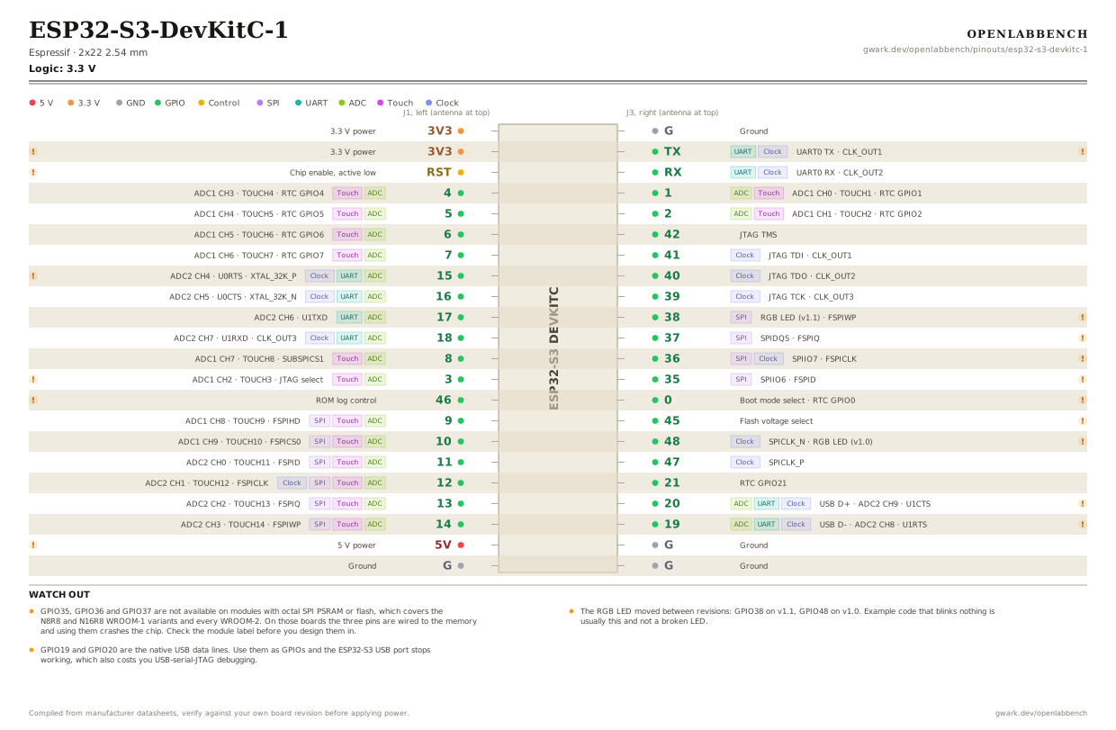
Fig. 1. ESP32-S3-DevKitC-1, 2x22 2.54 mm. Hover or tap a signal to light up every pin that carries it.
2.Watch out
- GPIO35, GPIO36 and GPIO37 are not available on modules with octal SPI PSRAM or flash, which covers the N8R8 and N16R8 WROOM-1 variants and every WROOM-2. On those boards the three pins are wired to the memory and using them crashes the chip. Check the module label before you design them in.
- The RGB LED moved between revisions: GPIO38 on v1.1, GPIO48 on v1.0. Example code that blinks nothing is usually this and not a broken LED.
- GPIO19 and GPIO20 are the native USB data lines. Use them as GPIOs and the ESP32-S3 USB port stops working, which also costs you USB-serial-JTAG debugging.
- Strapping pins are GPIO0 (BOOT), GPIO3, GPIO45 and GPIO46. They are sampled at reset, so what you hang on them decides how the chip boots. GPIO0 is the one wired to the BOOT button.
- ADC2 channels are unusable while Wi-Fi is running. That takes out GPIO11 through GPIO20 for analog, so put anything you need to measure on ADC1, which is GPIO1 to GPIO10.
- There are two USB ports. The one marked UART goes through a CP2102 bridge and always works for flashing. The one marked USB is the chip's own, and it is the one that disappears if you repurpose GPIO19 and GPIO20.
- The three ways to power the board are mutually exclusive: the USB ports, the 5V and G pins, or the 3V3 and G pins. Feeding two at once is how regulators die.
- Pin 1 of each header is at the antenna end, which is the top of this diagram, with both USB connectors at the bottom.
3.Full pin reference
Every pin, alias and mapping. This is the table that prints.
Table 1. Pin assignments.
| Pin | Name | Also called | Functions | Notes |
|---|---|---|---|---|
| - | 3V3 | - | 3.3 V power | |
| - | 3V3 | - | 3.3 V power | Two 3V3 pins, both the same net. |
| - | RST | EN | Chip enable, active low | Pull low to reset. The RESET button is on this net. |
| - | 4ADCTouch | GPIO4 | ADC1 CH3, TOUCH4, RTC GPIO4 | |
| - | 5ADCTouch | GPIO5 | ADC1 CH4, TOUCH5, RTC GPIO5 | |
| - | 6ADCTouch | GPIO6 | ADC1 CH5, TOUCH6, RTC GPIO6 | |
| - | 7ADCTouch | GPIO7 | ADC1 CH6, TOUCH7, RTC GPIO7 | |
| - | 15ADCUARTClock | GPIO15 | ADC2 CH4, U0RTS, XTAL_32K_P | One half of the 32 kHz crystal pair if you fit one. |
| - | 16ADCUARTClock | GPIO16 | ADC2 CH5, U0CTS, XTAL_32K_N | |
| - | 17ADCUART | GPIO17 | ADC2 CH6, U1TXD | |
| - | 18ADCUARTClock | GPIO18 | ADC2 CH7, U1RXD, CLK_OUT3 | |
| - | 8ADCTouch | GPIO8 | ADC1 CH7, TOUCH8, SUBSPICS1 | |
| - | 3ADCTouch | GPIO3 | ADC1 CH2, TOUCH3, JTAG select | Strapping pin. Sampled at reset. |
| - | 46 | GPIO46 | ROM log control | Strapping pin. Decides whether the ROM bootloader prints over serial. |
| - | 9ADCTouchSPI | GPIO9 | ADC1 CH8, TOUCH9, FSPIHD | |
| - | 10ADCTouchSPI | GPIO10 | ADC1 CH9, TOUCH10, FSPICS0 | |
| - | 11ADCTouchSPI | GPIO11 | ADC2 CH0, TOUCH11, FSPID | |
| - | 12ADCTouchSPIClock | GPIO12 | ADC2 CH1, TOUCH12, FSPICLK | |
| - | 13ADCTouchSPI | GPIO13 | ADC2 CH2, TOUCH13, FSPIQ | |
| - | 14ADCTouchSPI | GPIO14 | ADC2 CH3, TOUCH14, FSPIWP | |
| - | 5V | - | 5 V power | In or out, but never while a USB cable is also feeding the board. |
| - | G | GND | Ground | |
| - | G | GND | Ground | |
| - | TXUARTClock | GPIO43, U0TXD | UART0 TX, CLK_OUT1 | The console port. Also reachable through the UART USB socket. |
| - | RXUARTClock | GPIO44, U0RXD | UART0 RX, CLK_OUT2 | |
| - | 1ADCTouch | GPIO1 | ADC1 CH0, TOUCH1, RTC GPIO1 | |
| - | 2ADCTouch | GPIO2 | ADC1 CH1, TOUCH2, RTC GPIO2 | |
| - | 42 | GPIO42, MTMS | JTAG TMS | |
| - | 41Clock | GPIO41, MTDI | JTAG TDI, CLK_OUT1 | |
| - | 40Clock | GPIO40, MTDO | JTAG TDO, CLK_OUT2 | |
| - | 39Clock | GPIO39, MTCK | JTAG TCK, CLK_OUT3 | |
| - | 38SPI | GPIO38 | RGB LED (v1.1), FSPIWP | Drives the on-board addressable LED on v1.1. On v1.0 that job belongs to GPIO48. |
| - | 37SPI | GPIO37 | SPIDQS, FSPIQ | Not available on octal PSRAM or flash modules. |
| - | 36SPIClock | GPIO36 | SPIIO7, FSPICLK | Not available on octal PSRAM or flash modules. |
| - | 35SPI | GPIO35 | SPIIO6, FSPID | Not available on octal PSRAM or flash modules. |
| - | 0 | GPIO0, BOOT | Boot mode select, RTC GPIO0 | Strapping pin, and the BOOT button. Low at reset enters the download bootloader. |
| - | 45 | GPIO45 | Flash voltage select | Strapping pin. It picks the SPI flash supply voltage at reset. |
| - | 48Clock | GPIO48 | SPICLK_N, RGB LED (v1.0) | Drives the RGB LED on v1.0 boards only. |
| - | 47Clock | GPIO47 | SPICLK_P | |
| - | 21 | GPIO21 | RTC GPIO21 | |
| - | 20ADCUARTClock | GPIO20, USB_D+ | USB D+, ADC2 CH9, U1CTS | Native USB. Reusing it as a GPIO removes the USB port and the JTAG that rides on it. |
| - | 19ADCUARTClock | GPIO19, USB_D- | USB D-, ADC2 CH8, U1RTS | Native USB. Same warning as GPIO20. |
| - | G | GND | Ground | |
| - | G | GND | Ground |
Found a wrong pin? The whole board is one file, data/boards/esp32-s3-devkitc-1.json.