NXP · Dev board
NXP FRDM-K64F
120 MHz Cortex-M4F with Ethernet, an accelerometer, a microSD slot and an on-board debugger, in the Arduino Uno R3 footprint, but it is a 3.3 V board.
- Logic level
- 3.3 V, not 5 V tolerant
- Package
- Arduino Uno R3 form factor, 81 x 53 mm
1.Pinout diagram
Highlight a signalhover to preview, click to keep
Digital headers
Power + Analog headers
Pin detail
Hover a pin for its mappings and gotchas. Click to keep it here.
- Logic level
- 3.3 V, not 5 V tolerant
- Package
- Arduino Uno R3 form factor, 81 x 53 mm
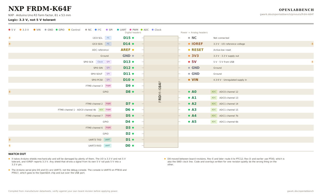
Fig. 1. NXP FRDM-K64F, Arduino Uno R3 form factor, 81 x 53 mm. Hover or tap a signal to light up every pin that carries it.
2.Watch out
- It takes Arduino shields mechanically and will be damaged by plenty of them. The I/O is 3.3 V and not 5 V tolerant, and IOREF reports 3.3 V. Any shield that drives a signal from its own 5 V rail puts 5 V into a 3.3 V pin.
- D8 moved between board revisions. Rev E and later route it to PTC12; Rev D and earlier use PTA0, which is also the SWD clock line. Code and overlays written for one revision quietly do the wrong thing on the other.
- The Arduino serial pins D0 and D1 are UART3, not the debug console. The console is UART0 on PTB16 and PTB17, which goes to the OpenSDA chip and out over the USB port.
- UART3 is shared three ways: the D0/D1 header pins, the Bluetooth HCI header, and the Ethernet IEEE 1588 timer pins PTC16 to PTC19. Enabling Ethernet and the header serial together will not work.
- I2C0 on D14 and D15 is shared with the on-board FXOS8700 accelerometer and magnetometer at address 0x1D. It is a real bus with real pull-ups, so extra devices are fine as long as the address does not clash.
- SPI0 follows the Arduino convention: D10 is chip select, D11 is MOSI, D12 is MISO, D13 is SCK. The microSD slot is on the same bus.
- OpenSDAv2 gives you drag-and-drop flashing over USB mass storage, a CMSIS-DAP debug interface and a serial console on one cable. No external programmer needed.
- There are extra pins outside the Arduino footprint, on the outer rows of the same headers, carrying the rest of the Ethernet and the CAN pins. Those are not shown here.
3.Register configuration
Turning a pin on the diagram into a configured pin.
Blink the red LED on PTB22
CMSIS device headers
#include "MK64F12.h"

/* Kinetis splits this in two: SIM gates the clock, PORT muxes the
   pin, GPIO drives it. Miss the SIM line and the PORT writes do
   nothing at all. */
SIM->SCGC5 |= SIM_SCGC5_PORTB_MASK;

PORTB->PCR[22] = PORT_PCR_MUX(1);     /* ALT1 = plain GPIO */

GPIOB->PDDR |= (1u << 22);            /* 1 = output */
GPIOB->PCOR  = (1u << 22);            /* clear, LED on  */
GPIOB->PSOR  = (1u << 22);            /* set,   LED off */
GPIOB->PTOR  = (1u << 22);            /* toggle */
PORT and GPIO are separate peripherals with separate clock gates. Writing PCR without first setting the SIM_SCGC5 bit silently does nothing, which looks exactly like a dead pin.
4.Full pin reference
Every pin, alias and mapping. This is the table that prints.
Table 1. Pin assignments.
| Pin | Name | Also called | Functions | Notes |
|---|---|---|---|---|
| - | D15I²C | SCL, PTE24 | I2C0 SCL | Shared with the on-board FXOS8700 accelerometer and magnetometer. |
| - | D14I²C | SDA, PTE25 | I2C0 SDA | Shared with the on-board FXOS8700. |
| - | AREF | - | ADC reference | |
| - | GND | - | Ground | |
| - | D13SPIClock | PTD1, SCK | SPI0 SCK | |
| - | D12SPI | PTD3, MISO | SPI0 SIN | |
| - | D11SPI | PTD2, MOSI | SPI0 SOUT | |
| - | D10SPI | PTD0, SS | SPI0 PCS0 | |
| - | D9PWM | PTC4 | FTM0 channel 3 | |
| - | D8 | PTC12 | GPIO | Rev E and later is PTC12. Rev D and earlier is PTA0, which is also the SWD clock. Check the board revision before trusting this one. |
| - | D7PWM | PTC3 | FTM0 channel 2 | |
| - | D6PWMADC | PTC2 | FTM0 channel 1, ADC0 channel 4b | |
| - | D5PWM | PTA2 | FTM0 channel 7 | |
| - | D4 | PTB23 | GPIO | |
| - | D3PWM | PTA1 | FTM0 channel 6 | |
| - | D2 | PTB9 | GPIO | |
| - | D1UART | PTC17, TX | UART3 TXD | UART3 also goes to the Bluetooth HCI header and to the Ethernet 1588 timers. Only one at a time. |
| - | D0UART | PTC16, RX | UART3 RXD | Not the console. The OpenSDA debug serial is UART0 on PTB16 and PTB17, which are not on this header. |
| - | NC | - | Not connected | |
| - | IOREF3.3 V | - | I/O reference voltage | 3.3 V, not 5 V. A shield that reads this will configure itself correctly; one that ignores it will not. |
| - | RESET | - | Active-low reset | |
| - | 3V33.3 V | - | 3.3 V supply out | |
| - | 5V5 V | - | 5 V from USB | Supply rail only. No I/O pin on this board is 5 V tolerant. |
| - | GND | - | Ground | |
| - | GND | - | Ground | |
| - | VIN4.3-9 V | - | Unregulated supply in | |
| - | A0ADC | PTB2 | ADC0 channel 12 | |
| - | A1ADC | PTB3 | ADC0 channel 13 | |
| - | A2ADC | PTB10 | ADC1 channel 14 | |
| - | A3ADC | PTB11 | ADC1 channel 15 | |
| - | A4ADC | PTC11 | ADC1 channel 7b | |
| - | A5ADC | PTC10 | ADC1 channel 6b |
Primary sources
Found a wrong pin? The whole board is one file, data/boards/frdm-k64f.json.