Avia Semiconductor · Integrated circuit
HX711 Load Cell Amplifier
A 24-bit ADC built for bridge sensors, with the gain and the reference already inside. What turns four strain gauge wires into a weight.
- Logic level
- 2.6-5.5 V
- Package
- SOP-16
1.Pinout diagram
Highlight a signalhover to preview, click to keep
Pins 1-8
Pins 9-16
Pin detail
Hover a pin for its mappings and gotchas. Click to keep it here.
- Logic level
- 2.6-5.5 V
- Package
- SOP-16
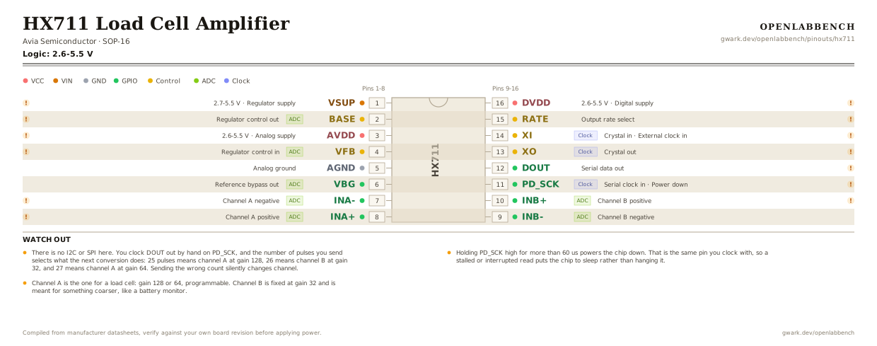
Fig. 1. HX711 Load Cell Amplifier, SOP-16. Hover or tap a signal to light up every pin that carries it.
2.Watch out
- There is no I2C or SPI here. You clock DOUT out by hand on PD_SCK, and the number of pulses you send selects what the next conversion does: 25 pulses means channel A at gain 128, 26 means channel B at gain 32, and 27 means channel A at gain 64. Sending the wrong count silently changes channel.
- Holding PD_SCK high for more than 60 us powers the chip down. That is the same pin you clock with, so a stalled or interrupted read puts the chip to sleep rather than hanging it.
- Channel A is the one for a load cell: gain 128 or 64, programmable. Channel B is fixed at gain 32 and is meant for something coarser, like a battery monitor.
- Full-scale differential input is only +/-0.5 x AVDD / gain, so at 5 V and gain 128 that is about +/-20 mV. A load cell's output is in that range, which is exactly the point, and anything larger clips immediately.
- The inputs have to sit between AGND + 1.2 V and AVDD - 1.3 V. A bridge excited from the full rail puts its outputs near mid-supply, which is comfortably inside that, but a single-ended sensor referenced to ground is not.
- RATE picks 10 Hz or 80 Hz. 10 Hz is the quieter one and is what most modules hardwire. 80 Hz costs you roughly a bit and a half of noise-free resolution.
- XI low selects the on-chip oscillator, which is what you want unless you are feeding it a crystal. BASE and XO are left unconnected when the on-board regulator and the crystal are unused.
- The 24 bits are real but the useful ones are fewer. Load cell work lives or dies on mechanical mounting and temperature, not on the ADC.
3.Minimum circuit with the internal oscillator
What has to go around the chip before it will run.
| Part | Between | Why |
|---|---|---|
| 0.1 uF ceramic | AVDD (3) to GND | Analog supply decoupling. This rail excites the bridge and sets the reference, so noise on it lands directly in the reading. |
| 0.1 uF ceramic | DVDD (16) to GND | Digital supply decoupling, kept separate from the analog side so clocking does not modulate the measurement. |
| Feedback link | VFB (4) to GND | VFB goes to AGND when the on-chip regulator is unused, which the datasheet states outright. Floating, the regulator control loop has no input. |
| Oscillator link | XI (14) to GND | XI low selects the internal oscillator. Only tie it high or drive it if you are supplying a clock. |
| Rate link | RATE (15) to GND | RATE low gives 10 samples per second, the quieter of the two. High gives 80. |
| Load cell bridge | INA+ (8) to INA- (7) | The sensor itself, across channel A. Its two output wires go here, and its excitation pair goes to AVDD and AGND. |
BASE and XO are left unconnected when the on-board regulator and crystal are unused. The bridge is excited from AVDD and AGND, which is why the reference tracks the excitation and the reading does not drift when the supply does.
4.Full pin reference
Every pin, alias and mapping. This is the table that prints.
Table 2. Pin assignments.
| Pin | Name | Also called | Functions | Notes |
|---|---|---|---|---|
| 1 | VSUP2.7-5.5 V | - | Regulator supply | Feeds the optional on-chip regulator, not the chip's own logic. |
| 2 | BASEADC | - | Regulator control out | Leave unconnected when the regulator is unused. |
| 3 | AVDD2.6-5.5 V | - | Analog supply | Also the bridge excitation and the reference. Everything measured is a ratio of this. |
| 4 | VFBADC | - | Regulator control in | To AGND when the regulator is unused. |
| 5 | AGND | - | Analog ground | |
| 6 | VBGADC | - | Reference bypass out | |
| 7 | INA-ADC | - | Channel A negative | Must stay between AGND + 1.2 V and AVDD - 1.3 V. |
| 8 | INA+ADC | - | Channel A positive | The load cell channel. Gain 128 or 64. |
| 9 | INB-ADC | - | Channel B negative | |
| 10 | INB+ADC | - | Channel B positive | Fixed gain of 32. Meant for something coarser than a load cell. |
| 11 | PD_SCKClock | - | Serial clock in, Power down | Clock it 25, 26 or 27 times to pick the next channel and gain. Held high over 60 us, it powers the chip down. |
| 12 | DOUT | - | Serial data out | Goes low when a conversion is ready, which is how you poll it. |
| 13 | XOClock | - | Crystal out | Leave unconnected when no crystal is fitted. |
| 14 | XIClock | - | Crystal in, External clock in | Low selects the on-chip oscillator. |
| 15 | RATE | - | Output rate select | Low is 10 Hz, high is 80 Hz. |
| 16 | DVDD2.6-5.5 V | - | Digital supply | Sets the logic level of DOUT, so match it to the microcontroller. |
Looking for a substitute?
Primary sources
Found a wrong pin? The whole board is one file, data/boards/hx711.json.