Intersil / Analog Devices / many · Integrated circuit
ICL7660 Charge Pump Inverter
Turns +5 V into -5 V with two capacitors and no inductor. The cheapest way to get a negative rail for an op-amp on a single-supply board.
- Logic level
- 1.5-10 V
- Package
- PDIP-8 / SOIC-8
1.Pinout diagram
Highlight a signalhover to preview, click to keep
Pins 1-4
Pins 5-8
Pin detail
Hover a pin for its mappings and gotchas. Click to keep it here.
- Logic level
- 1.5-10 V
- Package
- PDIP-8 / SOIC-8
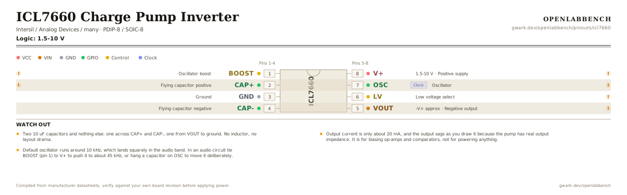
Fig. 1. ICL7660 Charge Pump Inverter, PDIP-8. Hover or tap a signal to light up every pin that carries it.
2.Watch out
- Two 10 uF capacitors and nothing else: one across CAP+ and CAP-, one from VOUT to ground. No inductor, no layout drama.
- Output current is only about 20 mA, and the output sags as you draw it because the pump has real output impedance. It is for biasing op-amps and comparators, not for powering anything.
- Default oscillator runs around 10 kHz, which lands squarely in the audio band. In an audio circuit tie BOOST (pin 1) to V+ to push it to about 45 kHz, or hang a capacitor on OSC to move it deliberately.
- LV (pin 6) should be grounded below 3.5 V supply and left open above it. Getting this backwards is the usual reason a 7660 works at 5 V and not at 3 V, or latches up at 9 V.
- It can also double a voltage instead of inverting it, by rearranging the capacitors. The datasheet has the connection; it is not the default.
- Absolute maximum is 10.5 V on the original ICL7660. The LM2662 and MAX1044 variants take more and deliver more current; check the exact part before applying 12 V.
3.Negative supply
What has to go around the chip before it will run.
| Part | Between | Why |
|---|---|---|
| 10 uF | CAP+ (2) to CAP- (4) | The charge pump capacitor. This is the one that actually moves the charge across. |
| 10 uF | VOUT (5) to GND | Reservoir on the output. Without it the negative rail is a sawtooth, not a supply. |
| Wire linkoptional | LV (6) to GND | LV bypasses the internal regulator below 3.5 V. Above 3.5 V it must be left open or the part can latch up. |
| 100 nFoptional | V+ (8) to GND | Supply decoupling at the pin. |
Output impedance is around 55 ohms, so the negative rail sags under load: at 20 mA you lose more than a volt. It is a bias supply for op-amps and LCD contrast, not a power rail.
4.Full pin reference
Every pin, alias and mapping. This is the table that prints.
Table 2. Pin assignments.
| Pin | Name | Also called | Functions | Notes |
|---|---|---|---|---|
| 1 | BOOST | NC on some parts | Oscillator boost | Tie to V+ to raise the oscillator to about 45 kHz, out of the audio band. |
| 2 | CAP+ | - | Flying capacitor positive | 10 uF between CAP+ and CAP-. |
| 3 | GND | - | Ground | |
| 4 | CAP- | - | Flying capacitor negative | |
| 5 | VOUT-V+ approx | - | Negative output | Roughly minus the supply, minus the droop under load. 10 uF to ground here. |
| 6 | LV | - | Low voltage select | Ground it below 3.5 V supply, leave open above. The wrong choice is why it works at one rail and not another. |
| 7 | OSCClock | - | Oscillator | A capacitor here slows the pump; an external clock overrides it. |
| 8 | V+1.5-10 V | - | Positive supply | 10.5 V absolute maximum on the original part. |
Primary sources
Found a wrong pin? The whole board is one file, data/boards/icl7660.json.