TI / ON / many · Integrated circuit
LM324 Quad Op-Amp
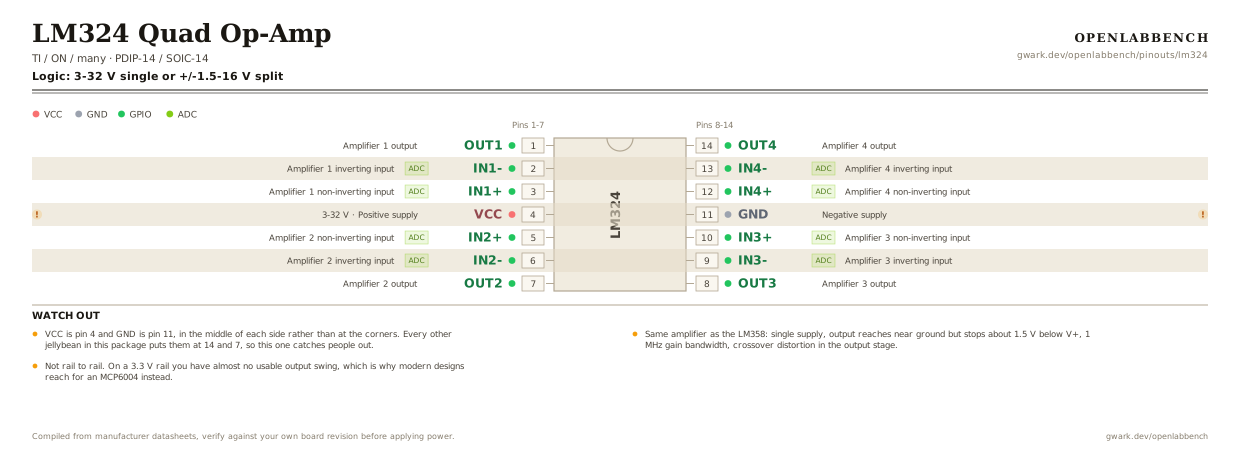
Four LM358s in a DIP-14, and a completely different pin arrangement from the dual. Note the supply pins are not at the corners.
- Logic level
- 3-32 V single or +/-1.5-16 V split
- Package
- PDIP-14 / SOIC-14
1.Pinout diagram
Highlight a signalhover to preview, click to keep
Pins 1-7
LM324
Pins 8-14
Pin detail
Hover a pin for its mappings and gotchas. Click to keep it here.
- Logic level
- 3-32 V single or +/-1.5-16 V split
- Package
- PDIP-14 / SOIC-14
Fig. 1. LM324 Quad Op-Amp, PDIP-14. Hover or tap a signal to light up every pin that carries it.
2.Watch out
- VCC is pin 4 and GND is pin 11, in the middle of each side rather than at the corners. Every other jellybean in this package puts them at 14 and 7, so this one catches people out.
- Same amplifier as the LM358: single supply, output reaches near ground but stops about 1.5 V below V+, 1 MHz gain bandwidth, crossover distortion in the output stage.
- Not rail to rail. On a 3.3 V rail you have almost no usable output swing, which is why modern designs reach for an MCP6004 instead.
- The LM339 is the comparator in this package and is NOT pin compatible with the LM324. Its supply pins are 3 and 12, and its outputs are open collector.
- Unused amplifiers should be wired as unity-gain followers with the input tied to a mid-rail reference, not left floating.
3.Single-supply follower
What has to go around the chip before it will run.
| Part | Between | Why |
|---|---|---|
| Wire link | OUT1 (1) to IN1- (2) | Output back to the inverting input. One of the four amplifiers wired as a unity-gain buffer. |
| 100 kOhmoptional | IN1+ (3) to VCC | Half-rail bias, so a single-supply input sits in a range the amplifier can follow. |
| 100 kOhmoptional | IN1+ (3) to GND | The lower half of the same divider. |
| 100 nF | VCC (4) to GND | Supply decoupling at the pin. |
Same die family as the LM358, with four amplifiers instead of two. The output cannot reach the positive rail, so a follower biased at exactly half supply clips the top of a large signal first.
4.Full pin reference
Every pin, alias and mapping. This is the table that prints.
Table 2. Pin assignments.
| Pin | Name | Also called | Functions | Notes |
|---|---|---|---|---|
| 1 | OUT1 | - | Amplifier 1 output | |
| 2 | IN1-ADC | - | Amplifier 1 inverting input | |
| 3 | IN1+ADC | - | Amplifier 1 non-inverting input | |
| 4 | VCC3-32 V | - | Positive supply | Pin 4, not pin 14. 100 nF to ground here. |
| 5 | IN2+ADC | - | Amplifier 2 non-inverting input | |
| 6 | IN2-ADC | - | Amplifier 2 inverting input | |
| 7 | OUT2 | - | Amplifier 2 output | |
| 8 | OUT3 | - | Amplifier 3 output | |
| 9 | IN3-ADC | - | Amplifier 3 inverting input | |
| 10 | IN3+ADC | - | Amplifier 3 non-inverting input | |
| 11 | GND | V- | Negative supply | Pin 11, not pin 7. |
| 12 | IN4+ADC | - | Amplifier 4 non-inverting input | |
| 13 | IN4-ADC | - | Amplifier 4 inverting input | |
| 14 | OUT4 | - | Amplifier 4 output |
Primary sources
Found a wrong pin? The whole board is one file, data/boards/lm324.json.