TI / ON / many · Integrated circuit
LM358 Dual Op-Amp
The default jellybean op-amp: two channels, runs from a single supply, and cannot reach either rail.
- Logic level
- 3-32 V single or +/-1.5-16 V split
- Package
- PDIP-8 / SOIC-8
1.Pinout diagram
Highlight a signalhover to preview, click to keep
Pins 1-4
Pins 5-8
Pin detail
Hover a pin for its mappings and gotchas. Click to keep it here.
- Logic level
- 3-32 V single or +/-1.5-16 V split
- Package
- PDIP-8 / SOIC-8
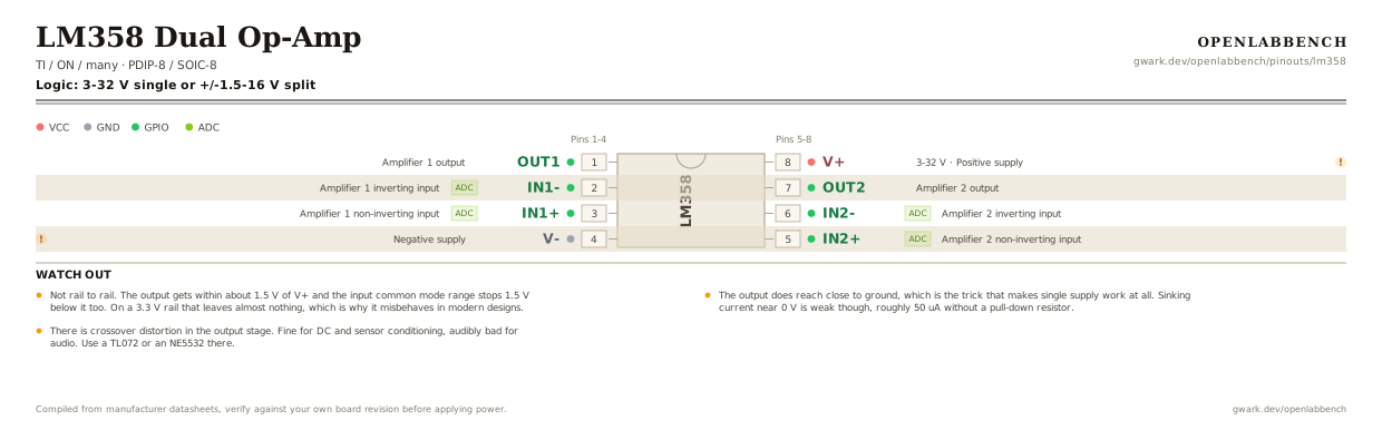
Fig. 1. LM358 Dual Op-Amp, PDIP-8. Hover or tap a signal to light up every pin that carries it.
2.Watch out
- Not rail to rail. The output gets within about 1.5 V of V+ and the input common mode range stops 1.5 V below it too. On a 3.3 V rail that leaves almost nothing, which is why it misbehaves in modern designs.
- The output does reach close to ground, which is the trick that makes single supply work at all. Sinking current near 0 V is weak though, roughly 50 uA without a pull-down resistor.
- There is crossover distortion in the output stage. Fine for DC and sensor conditioning, audibly bad for audio. Use a TL072 or an NE5532 there.
- 1 MHz gain bandwidth. At a gain of 100 you have 10 kHz of bandwidth left, and no more.
- The LM393 comparator shares this package and pin arrangement but has an open collector output. The two look identical on a board and are not interchangeable.
- Pin 4 is the negative supply, which is ground in a single supply circuit. Pin 8 is V+. That is the opposite corner pair from most DIP-8 logic.
3.Single-supply follower
What has to go around the chip before it will run.
| Part | Between | Why |
|---|---|---|
| Wire link | OUT1 (1) to IN1- (2) | Output straight back to the inverting input. Unity gain, the simplest useful configuration. |
| 100 kOhmoptional | IN1+ (3) to VCC | Half-rail bias. On a single supply the input has to sit somewhere the amplifier can actually reach. |
| 100 kOhmoptional | IN1+ (3) to GND | The lower half of the same divider. |
| 1 uFoptional | IN1+ (3) to GND | Stops supply noise riding straight through the bias divider into the input. |
| 100 nF | V+ (8) to GND | Supply decoupling at the pin. |
The input range includes ground but the output does not: it only swings down to about 20 mV above the negative rail, and up to about 1.5 V below the positive one. The LM358 is not rail to rail, whatever the breakout board says.
4.Full pin reference
Every pin, alias and mapping. This is the table that prints.
Table 2. Pin assignments.
| Pin | Name | Also called | Functions | Notes |
|---|---|---|---|---|
| 1 | OUT1 | OUTA | Amplifier 1 output | |
| 2 | IN1-ADC | INA- | Amplifier 1 inverting input | |
| 3 | IN1+ADC | INA+ | Amplifier 1 non-inverting input | |
| 4 | V- | GND, VEE | Negative supply | Ground in a single supply circuit. |
| 5 | IN2+ADC | INB+ | Amplifier 2 non-inverting input | |
| 6 | IN2-ADC | INB- | Amplifier 2 inverting input | |
| 7 | OUT2 | OUTB | Amplifier 2 output | |
| 8 | V+3-32 V | - | Positive supply | 100 nF to ground at the pin. |
Looking for a substitute?
Primary sources
Found a wrong pin? The whole board is one file, data/boards/lm358.json.