Maxim / TI / many · Integrated circuit
MAX485 RS-485 Transceiver
Half-duplex RS-485 driver and receiver, the usual way to get Modbus or a long serial run off a microcontroller.
- Logic level
- 5 V (MAX3485 is the 3.3 V part)
- Package
- PDIP-8 / SOIC-8
1.Pinout diagram
Highlight a signalhover to preview, click to keep
Pins 1-4
MAX485
Pins 5-8
Pin detail
Hover a pin for its mappings and gotchas. Click to keep it here.
- Logic level
- 5 V (MAX3485 is the 3.3 V part)
- Package
- PDIP-8 / SOIC-8
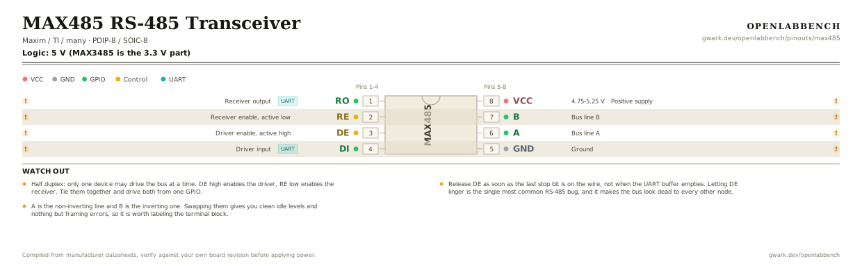
Fig. 1. MAX485 RS-485 Transceiver, PDIP-8. Hover or tap a signal to light up every pin that carries it.
2.Watch out
- Half duplex: only one device may drive the bus at a time. DE high enables the driver, RE low enables the receiver. Tie them together and drive both from one GPIO.
- Release DE as soon as the last stop bit is on the wire, not when the UART buffer empties. Letting DE linger is the single most common RS-485 bug, and it makes the bus look dead to every other node.
- A is the non-inverting line and B is the inverting one. Swapping them gives you clean idle levels and nothing but framing errors, so it is worth labeling the terminal block.
- Terminate with 120 ohm across A and B at each end of the cable, and only at the ends. Mid-run terminators load the bus.
- Idle bias matters: with every driver off the bus floats and receivers see noise as start bits. Add a pull-up on A and a pull-down on B, around 680 ohm, somewhere on the segment.
- The plain MAX485 is a full unit load, so 32 nodes. MAX487 and friends are quarter unit load and reach 128.
- This chip is 5 V. Driving its DI from 3.3 V logic works, but RO comes back at 5 V and needs a divider into a 3.3 V micro. The MAX3485 avoids the whole problem.
3.Half-duplex RS-485 node
What has to go around the chip before it will run.
| Part | Between | Why |
|---|---|---|
| 120 Ohmoptional | A (6) to B (7) | Termination, and only at the two physical ends of the cable. Mid-run terminators load the bus. |
| 680 Ohmoptional | A (6) to VCC | Idle bias, so receivers see a defined state when no driver is enabled. |
| 680 Ohmoptional | B (7) to GND | The other half of the idle bias pair. |
| Wire link | RE (2) to DE (3) | Ties receive enable to drive enable so one GPIO controls direction. |
| 100 nF | VCC (8) to GND | Supply decoupling at the pin. |
Ground must be common across the bus as well as the differential pair. A and B alone work on the bench and fail over a long run.
4.Full pin reference
Every pin, alias and mapping. This is the table that prints.
Table 2. Pin assignments.
| Pin | Name | Also called | Functions | Notes |
|---|---|---|---|---|
| 1 | ROUART | R, RXD | Receiver output | Goes to your microcontroller's RX. |
| 2 | RE | /RE, nRE | Receiver enable, active low | Usually tied to DE and driven by one GPIO. |
| 3 | DE | - | Driver enable, active high | High to transmit. Drop it the moment the last stop bit is out. |
| 4 | DIUART | D, TXD | Driver input | Goes to your microcontroller's TX. |
| 5 | GND | - | Ground | The bus needs a common ground reference as well as the differential pair. |
| 6 | A | D+, non-inverting | Bus line A | Non-inverting. Idles high relative to B. |
| 7 | B | D-, inverting | Bus line B | Inverting. |
| 8 | VCC4.75-5.25 V | - | Positive supply | 100 nF at the pin. |
Looking for a substitute?
Primary sources
Found a wrong pin? The whole board is one file, data/boards/max485.json.