Microchip · Integrated circuit
MCP23017 I2C I/O Expander
Sixteen real GPIOs over two wires, with direction, pull-ups and interrupts per pin. The PCF8574 grown up and given a register map.
- Logic level
- 1.8-5.5 V
- Package
- SPDIP-28 / SOIC-28 / SSOP-28
1.Pinout diagram
Highlight a signalhover to preview, click to keep
Pins 1-14
MCP23017
Pins 15-28
Pin detail
Hover a pin for its mappings and gotchas. Click to keep it here.
- Logic level
- 1.8-5.5 V
- Package
- SPDIP-28 / SOIC-28 / SSOP-28
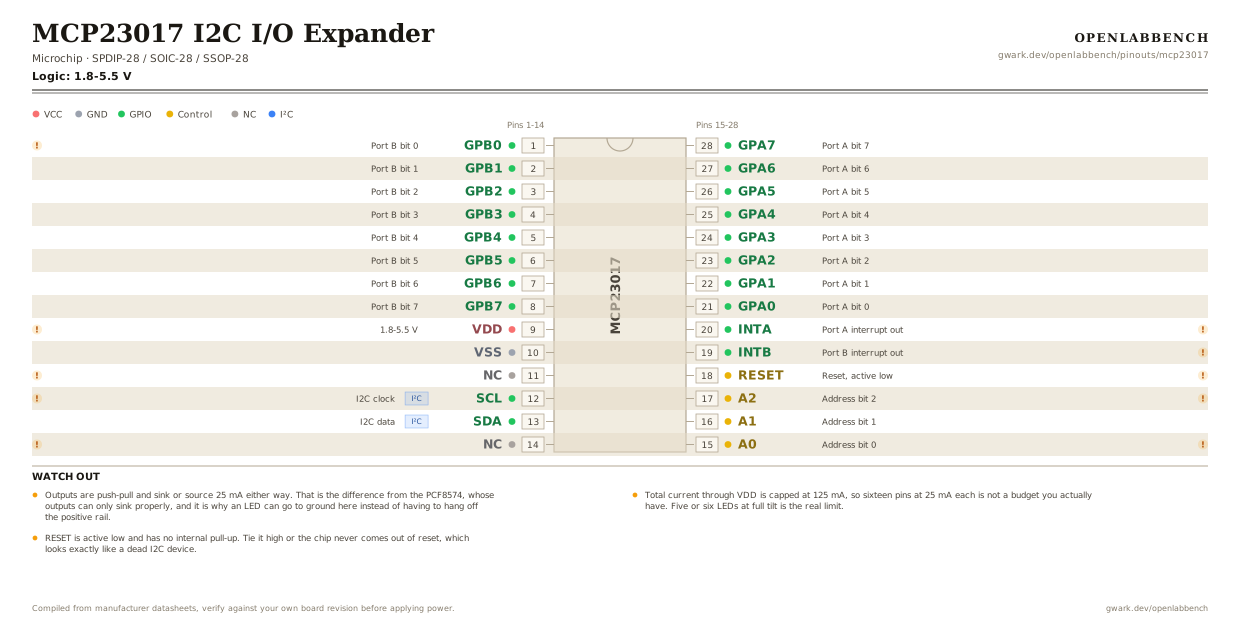
Fig. 1. MCP23017 I2C I/O Expander, SPDIP-28. Hover or tap a signal to light up every pin that carries it.
2.Watch out
- Outputs are push-pull and sink or source 25 mA either way. That is the difference from the PCF8574, whose outputs can only sink properly, and it is why an LED can go to ground here instead of having to hang off the positive rail.
- Total current through VDD is capped at 125 mA, so sixteen pins at 25 mA each is not a budget you actually have. Five or six LEDs at full tilt is the real limit.
- RESET is active low and has no internal pull-up. Tie it high or the chip never comes out of reset, which looks exactly like a dead I2C device.
- Two independent interrupt pins, INTA for port A and INTB for port B, with per-pin enables and a choice between comparing against the previous value or against a configured default. They can be tied together in software with the MIRROR bit.
- The pull-ups are 100 kOhm, configurable per pin, and they are the reason this part is pleasant for reading buttons. The PCF8574 has nothing equivalent.
- A0, A1 and A2 give addresses 0x20 to 0x27, which collides with the PCF8574's range. Both on one bus means picking different addresses on purpose.
- Pins 11 and 14 are not connected here. On the MCP23S17, the SPI version in the same package, they are CS and SO.
- There are two register orderings, picked by the BANK bit, and libraries disagree about which they assume. If every register you touch is off by one, that is why. BANK=0 is the power-up default.
3.Minimum circuit
What has to go around the chip before it will run.
| Part | Between | Why |
|---|---|---|
| 0.1 uF ceramic | VDD (9) to GND | Supply decoupling at the pin. Sixteen outputs changing together is a step the supply has to absorb. |
| Reset link | RESET (18) to VCC | RESET is active low with no internal pull-up. Held low, the chip never responds and looks like it is not on the bus. |
| 4.7 kOhm | SDA (13) to VCC | I2C pull-up on SDA. The bus is open drain and cannot pull itself high. |
| 4.7 kOhm | SCL (12) to VCC | I2C pull-up on SCL. One pair per bus, not per device. |
| Address link | A0 (15) to GND | A0 tied low. Address pins are TTL inputs with no pull-up, so each needs a wire. |
| Address link | A1 (16) to GND | A1 tied low. Tie it high instead and the address goes up by 2. |
| Address link | A2 (17) to GND | A2 tied low. All three low puts the chip at 0x20. |
INTA and INTB are open drain by default and need their own pull-up if you use them. Nothing else is required: the GPIO pull-ups are inside the chip and switched on in software.
4.Full pin reference
Every pin, alias and mapping. This is the table that prints.
Table 2. Pin assignments.
| Pin | Name | Also called | Functions | Notes |
|---|---|---|---|---|
| 1 | GPB0 | - | Port B bit 0 | Push-pull, 25 mA either direction, with an optional 100 kOhm pull-up. |
| 2 | GPB1 | - | Port B bit 1 | |
| 3 | GPB2 | - | Port B bit 2 | |
| 4 | GPB3 | - | Port B bit 3 | |
| 5 | GPB4 | - | Port B bit 4 | |
| 6 | GPB5 | - | Port B bit 5 | |
| 7 | GPB6 | - | Port B bit 6 | |
| 8 | GPB7 | - | Port B bit 7 | |
| 9 | VDD1.8-5.5 V | - | - | 125 mA total through this pin, which is the real ceiling on how much the sixteen outputs can drive. |
| 10 | VSS | GND | - | |
| 11 | NC | - | - | CS on the SPI version, the MCP23S17. |
| 12 | SCLI²C | SCK | I2C clock | To 1.7 MHz. The datasheet's package drawing labels it SCK because it is shared with the SPI part. |
| 13 | SDAI²C | - | I2C data | |
| 14 | NC | - | - | SO on the SPI version, the MCP23S17. |
| 15 | A0 | - | Address bit 0 | TTL input, no pull-up. Tie it. |
| 16 | A1 | - | Address bit 1 | |
| 17 | A2 | - | Address bit 2 | All three low gives 0x20, all high gives 0x27. |
| 18 | RESET | /RESET | Reset, active low | No internal pull-up. Must be held high to run. |
| 19 | INTB | - | Port B interrupt out | Open drain by default. Configurable active high or low. |
| 20 | INTA | - | Port A interrupt out | Can be mirrored with INTB so either port triggers both. |
| 21 | GPA0 | - | Port A bit 0 | |
| 22 | GPA1 | - | Port A bit 1 | |
| 23 | GPA2 | - | Port A bit 2 | |
| 24 | GPA3 | - | Port A bit 3 | |
| 25 | GPA4 | - | Port A bit 4 | |
| 26 | GPA5 | - | Port A bit 5 | |
| 27 | GPA6 | - | Port A bit 6 | |
| 28 | GPA7 | - | Port A bit 7 |
Looking for a substitute?
Primary sources
Found a wrong pin? The whole board is one file, data/boards/mcp23017.json.