MOS / Rockwell / WDC · Microcontroller
MOS 6502
The 8-bit CPU behind the Apple II, C64, NES and BBC Micro, and still the usual first homebrew computer build.
- Logic level
- 5 V
- Package
- PDIP-40
1.Pinout diagram
Highlight a signalhover to preview, click to keep
Pins 1-20
6502
Pins 21-40
Pin detail
Hover a pin for its mappings and gotchas. Click to keep it here.
- Logic level
- 5 V
- Package
- PDIP-40
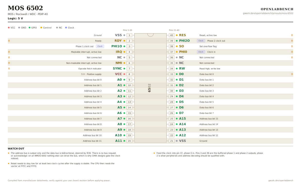
Fig. 1. MOS 6502, PDIP-40. Hover or tap a signal to light up every pin that carries it.
2.Watch out
- The address bus is output only and the data bus is bidirectional, steered by R/W. There is no bus request or acknowledge: on an NMOS 6502 nothing else can drive the bus, which is why DMA designs gate the clock instead.
- Feed the clock into pin 37, phase 0 in. Pins 3 and 39 are the buffered phase 1 and phase 2 outputs; phase 2 is what peripherals and address decoding should be qualified with.
- Reset needs to stay low for at least two clock cycles after the supply is stable. The CPU then reads the vector at FFFC and FFFD.
- Vectors live at the top of memory: NMI at FFFA, RESET at FFFC, IRQ and BRK at FFFE.
- IRQ is level sensitive and maskable with SEI. NMI is edge triggered and cannot be masked, so a noisy NMI line gives you interrupts you never asked for. Tie both high through a resistor if unused.
- The NMOS 6502 has no minimum clock speed restriction going up but will lose state if clocked too slowly. The CMOS W65C02 is fully static, so you can single-step it by hand with a debounced switch. That alone makes it the better part to learn on.
- On the W65C02 the unused pins change: pin 5 becomes ML, pin 36 becomes BE, and pin 38 becomes SOB. Pin 1 also becomes VPB on some variants.
3.Minimum circuit to run
What has to go around the chip before it will run.
| Part | Between | Why |
|---|---|---|
| Clock oscillator | PHI0 (37) to GND | A can oscillator or a crystal and gate. The NMOS part also has a minimum clock speed. |
| 10 kOhm | RES (40) to VCC | Reset pull-up, with a capacitor to ground for a power-on reset of at least two cycles. |
| 10 kOhm | IRQ (4) to VCC | Unused interrupt inputs must be held high or you get interrupts you never asked for. |
| 10 kOhm | NMI (6) to VCC | NMI is edge triggered and cannot be masked, so a floating pin is worse than IRQ. |
| 10 kOhm | RDY (2) to VCC | RDY is an active input and must be tied off. |
| 10 kOhm | SO (38) to VCC | Set-overflow is an active input and must be tied off. |
| 100 nF | VCC (8) to GND | Supply decoupling at the pin. |
Qualify address decoding with PHI2 (39), not with the raw address lines, or peripherals will see bus noise as accesses.
4.Full pin reference
Every pin, alias and mapping. This is the table that prints.
Table 2. Pin assignments.
| Pin | Name | Also called | Functions | Notes |
|---|---|---|---|---|
| 1 | VSS | - | Ground | |
| 2 | RDY | - | Ready | Pull low to freeze the CPU on a read cycle, for slow memory. Tie high if unused. |
| 3 | PHI1OClock | O1 OUT, phase 1 out | Phase 1 clock out | |
| 4 | IRQ | IRQB | Maskable interrupt, active low | Level sensitive. Tie high through 3k3 if unused. |
| 5 | NC | - | Not connected | ML (memory lock) on the W65C02. |
| 6 | NMI | NMIB | Non-maskable interrupt, active low | Edge triggered and unmaskable. Tie high through 3k3 if unused. |
| 7 | SYNC | - | Opcode fetch indicator | High during the first cycle of every instruction. The hook for single-stepping and for a hardware debugger. |
| 8 | VCC5 V | - | Positive supply | |
| 9 | A0 | - | Address bus bit 0 | |
| 10 | A1 | - | Address bus bit 1 | |
| 11 | A2 | - | Address bus bit 2 | |
| 12 | A3 | - | Address bus bit 3 | |
| 13 | A4 | - | Address bus bit 4 | |
| 14 | A5 | - | Address bus bit 5 | |
| 15 | A6 | - | Address bus bit 6 | |
| 16 | A7 | - | Address bus bit 7 | |
| 17 | A8 | - | Address bus bit 8 | |
| 18 | A9 | - | Address bus bit 9 | |
| 19 | A10 | - | Address bus bit 10 | |
| 20 | A11 | - | Address bus bit 11 | |
| 21 | VSS | - | Ground | |
| 22 | A12 | - | Address bus bit 12 | |
| 23 | A13 | - | Address bus bit 13 | |
| 24 | A14 | - | Address bus bit 14 | |
| 25 | A15 | - | Address bus bit 15 | |
| 26 | D7 | - | Data bus bit 7 | |
| 27 | D6 | - | Data bus bit 6 | |
| 28 | D5 | - | Data bus bit 5 | |
| 29 | D4 | - | Data bus bit 4 | |
| 30 | D3 | - | Data bus bit 3 | |
| 31 | D2 | - | Data bus bit 2 | |
| 32 | D1 | - | Data bus bit 1 | |
| 33 | D0 | - | Data bus bit 0 | The data bus runs D7 down to D0 as the pin numbers go up. |
| 34 | RW | R/W | Read high, write low | |
| 35 | NC | - | Not connected | |
| 36 | NC | - | Not connected | BE (bus enable) on the W65C02. |
| 37 | PHI0Clock | O0 IN, phase 0 in, CLK | Clock in | This is the pin your oscillator drives. |
| 38 | SO | S.O. | Set overflow flag | A falling edge sets V in the status register. Tie high if unused. |
| 39 | PHI2OClock | O2 OUT, phase 2 out | Phase 2 clock out | Qualify address decoding and peripheral chip selects with this. |
| 40 | RES | RESB, RESET | Reset, active low | Hold low for at least two cycles after the supply settles. |
Looking for a substitute?
Primary sources
Found a wrong pin? The whole board is one file, data/boards/mos-6502.json.