MOS / Rockwell / WDC · Integrated circuit
MOS 6522 VIA
Two 8-bit ports, two timers, a shift register and interrupt handling. The chip that turns a bare 6502 into a computer with I/O.
- Logic level
- 5 V
- Package
- PDIP-40
1.Pinout diagram
Highlight a signalhover to preview, click to keep
Pins 1-20
6522 VIA
Pins 21-40
Pin detail
Hover a pin for its mappings and gotchas. Click to keep it here.
- Logic level
- 5 V
- Package
- PDIP-40
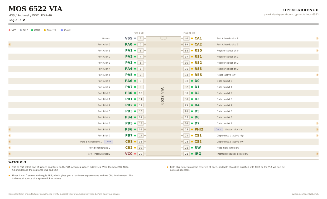
Fig. 1. MOS 6522 VIA, PDIP-40. Hover or tap a signal to light up every pin that carries it.
2.Watch out
- RS0 to RS3 select one of sixteen registers, so the VIA occupies sixteen addresses. Wire them to CPU A0 to A3 and decode the rest onto CS1 and CS2.
- Both chip selects must be asserted at once, and both should be qualified with PHI2 or the VIA will see bus noise as accesses.
- Timer 1 can free-run and toggle PB7, which gives you a hardware square wave with no CPU involvement. That is the usual source of a system tick or a tone.
- Timer 2 counts pulses on PB6 as well as time, so it doubles as an event counter.
- On the original NMOS 6522, reading Port A returns the pin states rather than the output register, so an output loaded down reads back wrong. Port B reads the register. The CMOS W65C22 fixes this.
- IRQ is open drain. Several VIAs and ACIAs share one interrupt line through a single pull-up, and the handler reads each chip's flag register to find out who shouted.
- The shift register has documented silicon bugs on the NMOS part and is best avoided; bit-bang through the ports instead, or use a W65C22.
- Ben Eater's 6502 build uses this chip, which is why it is back in production and easy to buy.
3.Minimum circuit
What has to go around the chip before it will run.
| Part | Between | Why |
|---|---|---|
| 100 nF | VCC (20) to GND | Supply decoupling at the pin. |
| 3.3 kOhm | IRQ (21) to VCC | IRQ is open drain so several peripherals can share one line. Nothing pulls it high on its own. |
| Wire linkoptional | CS1 (24) to VCC | Chip select 1 is active high. Tie it only on a bench rig where the VIA is the only device. |
| Wire linkoptional | CS2 (23) to GND | Chip select 2 is active low. In a real system both selects come from address decoding. |
RES (34) joins the system reset line, and PHI2 (25) must be the same clock the processor uses: every register access is timed from its falling edge.
4.Full pin reference
Every pin, alias and mapping. This is the table that prints.
Table 2. Pin assignments.
| Pin | Name | Also called | Functions | Notes |
|---|---|---|---|---|
| 1 | VSS | GND | Ground | |
| 2 | PA0 | - | Port A bit 0 | Reading Port A on the NMOS part returns the pin, not the output register. A loaded output reads back wrong. |
| 3 | PA1 | - | Port A bit 1 | |
| 4 | PA2 | - | Port A bit 2 | |
| 5 | PA3 | - | Port A bit 3 | |
| 6 | PA4 | - | Port A bit 4 | |
| 7 | PA5 | - | Port A bit 5 | |
| 8 | PA6 | - | Port A bit 6 | |
| 9 | PA7 | - | Port A bit 7 | |
| 10 | PB0 | - | Port B bit 0 | |
| 11 | PB1 | - | Port B bit 1 | |
| 12 | PB2 | - | Port B bit 2 | |
| 13 | PB3 | - | Port B bit 3 | |
| 14 | PB4 | - | Port B bit 4 | |
| 15 | PB5 | - | Port B bit 5 | |
| 16 | PB6 | - | Port B bit 6 | Timer 2 counts falling edges here, so it doubles as an event counter. |
| 17 | PB7 | - | Port B bit 7 | Timer 1 can toggle PB7 on its own, giving a hardware square wave with no CPU involvement. |
| 18 | CB1Clock | - | Port B handshake 1 | Shift register clock, and an interrupt source. |
| 19 | CB2 | - | Port B handshake 2 | Shift register data. |
| 20 | VCC5 V | - | Positive supply | 100 nF at the pin. |
| 21 | IRQ | /IRQ | Interrupt request, active low | Open drain, so several VIAs share one line through a pull-up. |
| 22 | RW | R/W | Read high, write low | |
| 23 | CS2 | /CS2 | Chip select 2, active low | |
| 24 | CS1 | - | Chip select 1, active high | Both selects must be asserted, and both should be qualified with PHI2. |
| 25 | PHI2Clock | O2, CLK | System clock in | Drive from the CPU phase 2 output. Every bus cycle is timed off this. |
| 26 | D7 | - | Data bus bit 7 | The data bus runs D7 down to D0 as the pin numbers rise, same as the 6502. |
| 27 | D6 | - | Data bus bit 6 | |
| 28 | D5 | - | Data bus bit 5 | |
| 29 | D4 | - | Data bus bit 4 | |
| 30 | D3 | - | Data bus bit 3 | |
| 31 | D2 | - | Data bus bit 2 | |
| 32 | D1 | - | Data bus bit 1 | |
| 33 | D0 | - | Data bus bit 0 | |
| 34 | RES | /RES, RESET | Reset, active low | Clears every register and puts both ports to input. |
| 35 | RS3 | - | Register select bit 3 | |
| 36 | RS2 | - | Register select bit 2 | |
| 37 | RS1 | - | Register select bit 1 | |
| 38 | RS0 | - | Register select bit 0 | RS0 to RS3 pick one of sixteen registers. Wire them to CPU A0 to A3. |
| 39 | CA2 | - | Port A handshake 2 | |
| 40 | CA1 | - | Port A handshake 1 | Input only, and an interrupt source. |
Primary sources
Found a wrong pin? The whole board is one file, data/boards/mos-6522.json.