MOS / Rockwell / WDC · Integrated circuit
MOS 6551 ACIA
Serial port for a 6502 system: a full UART with its own baud rate generator, so one crystal gives you every standard rate.
- Logic level
- 5 V
- Package
- PDIP-28
1.Pinout diagram
Highlight a signalhover to preview, click to keep
Pins 1-14
Pins 15-28
Pin detail
Hover a pin for its mappings and gotchas. Click to keep it here.
- Logic level
- 5 V
- Package
- PDIP-28
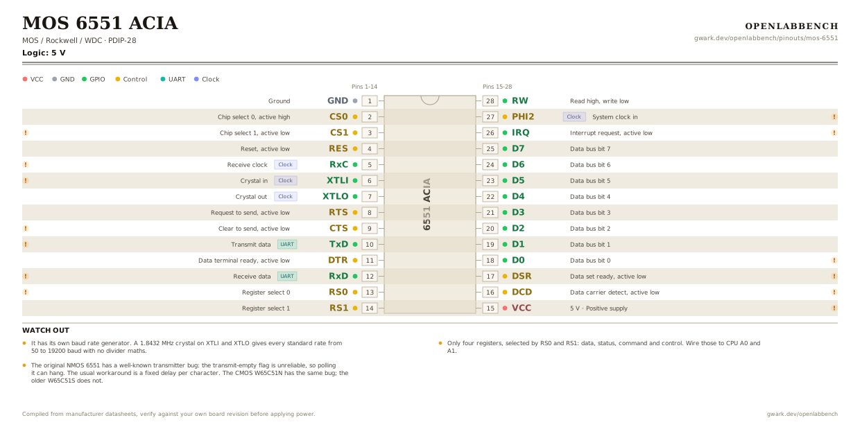
Fig. 1. MOS 6551 ACIA, PDIP-28. Hover or tap a signal to light up every pin that carries it.
2.Watch out
- It has its own baud rate generator. A 1.8432 MHz crystal on XTLI and XTLO gives every standard rate from 50 to 19200 baud with no divider maths.
- Only four registers, selected by RS0 and RS1: data, status, command and control. Wire those to CPU A0 and A1.
- The original NMOS 6551 has a well-known transmitter bug: the transmit-empty flag is unreliable, so polling it can hang. The usual workaround is a fixed delay per character. The CMOS W65C51N has the same bug; the older W65C51S does not.
- IRQ is open drain, so it shares one interrupt line with the VIA and anything else through a single pull-up.
- The modem control lines are real: RTS, CTS, DTR, DSR and DCD are all brought out, which is enough for proper hardware flow control.
- Output levels are TTL, not RS-232. A MAX232 or equivalent sits between this and a real serial port; for a modern USB adapter, wire TxD and RxD straight across.
- Pair it with a 6522 VIA and a 6502 and you have the classic three-chip computer.
3.Minimum circuit
What has to go around the chip before it will run.
| Part | Between | Why |
|---|---|---|
| 1.8432 MHz crystal | XTLI (6) to XTLO (7) | Divides to exact standard baud rates. Without it the internal rate generator has nothing to count. |
| 100 nF | VCC (15) to GND | Supply decoupling at the pin. |
| 3.3 kOhm | IRQ (26) to VCC | IRQ is open drain and shares a line with the other peripherals. |
Drive XTLI (6) directly from an external clock if you prefer, but then XTLO (7) must be left open. The NMOS part also has the famous transmit bug: the status register never reports the transmitter empty, so timing-based delays are the usual workaround.
4.Full pin reference
Every pin, alias and mapping. This is the table that prints.
Table 2. Pin assignments.
| Pin | Name | Also called | Functions | Notes |
|---|---|---|---|---|
| 1 | GND | VSS | Ground | |
| 2 | CS0 | - | Chip select 0, active high | |
| 3 | CS1 | /CS1 | Chip select 1, active low | Both selects must agree, and both should be qualified with PHI2. |
| 4 | RES | /RES, RESET | Reset, active low | |
| 5 | RxCClock | - | Receive clock | Output at 16x baud when using the internal generator; an input in external clock mode. |
| 6 | XTLIClock | - | Crystal in | 1.8432 MHz. That exact frequency is what makes every standard baud rate come out right. |
| 7 | XTLOClock | - | Crystal out | |
| 8 | RTS | /RTS | Request to send, active low | |
| 9 | CTS | /CTS | Clear to send, active low | Tie low if you are not using flow control, or the transmitter stays silent. |
| 10 | TxDUART | - | Transmit data | TTL level, not RS-232. |
| 11 | DTR | /DTR | Data terminal ready, active low | |
| 12 | RxDUART | - | Receive data | TTL level, not RS-232. |
| 13 | RS0 | - | Register select 0 | Wire RS0 and RS1 to CPU A0 and A1. |
| 14 | RS1 | - | Register select 1 | |
| 15 | VCC5 V | - | Positive supply | 100 nF at the pin. |
| 16 | DCD | /DCD | Data carrier detect, active low | Tie low if unused, or the receiver ignores incoming data. |
| 17 | DSR | /DSR | Data set ready, active low | Tie low if unused. |
| 18 | D0 | - | Data bus bit 0 | Unlike the 6502 and 6522, this bus runs D0 up to D7 as the pin numbers rise. |
| 19 | D1 | - | Data bus bit 1 | |
| 20 | D2 | - | Data bus bit 2 | |
| 21 | D3 | - | Data bus bit 3 | |
| 22 | D4 | - | Data bus bit 4 | |
| 23 | D5 | - | Data bus bit 5 | |
| 24 | D6 | - | Data bus bit 6 | |
| 25 | D7 | - | Data bus bit 7 | |
| 26 | IRQ | /IRQ | Interrupt request, active low | Open drain. Shares a line with the VIA through one pull-up. |
| 27 | PHI2Clock | O2, CLK | System clock in | From the CPU phase 2 output. |
| 28 | RW | R/W | Read high, write low |
Primary sources
Found a wrong pin? The whole board is one file, data/boards/mos-6551.json.