Texas Instruments / many · Integrated circuit
NE555 Timer
The timer that refuses to die. Monostable, astable or Schmitt comparator depending on how you wire the three resistor-divider taps. Pin 1 is bottom-left of the notch.
- Logic level
- 4.5-16 V
- Package
- PDIP-8 / SOIC-8
1.Pinout diagram
Highlight a signalhover to preview, click to keep
Pins 1-4
NE555
Pins 5-8
Pin detail
Hover a pin for its mappings and gotchas. Click to keep it here.
- Logic level
- 4.5-16 V
- Package
- PDIP-8 / SOIC-8
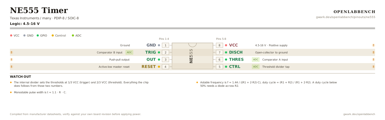
Fig. 1. NE555 Timer, PDIP-8. Hover or tap a signal to light up every pin that carries it.
2.Watch out
- The internal divider sets the thresholds at 1/3 VCC (trigger) and 2/3 VCC (threshold). Everything the chip does follows from those two numbers.
- Astable frequency is f ≈ 1.44 / ((R1 + 2·R2)·C), duty cycle = (R1 + R2) / (R1 + 2·R2). A duty cycle below 50% needs a diode across R2.
- Monostable pulse width is t ≈ 1.1 · R · C.
- RESET (pin 4) is active low and must be tied to VCC if unused, or the timer will not run.
- Decouple CONTROL (pin 5) to ground with 10 nF unless you are modulating it. Leaving it bare is the most common cause of a jittery 555.
- The bipolar NE555 pulls a current spike of 100-200 mA through its supply on every output transition. Put 100 nF across VCC and GND at the chip, and prefer the CMOS TLC555 near anything analog.
- The output is a totem pole that swings to within about 1.7 V of VCC on a bipolar 555, and does not reach ground either. Driving a MOSFET gate from a 5 V 555 is marginal; use the CMOS TLC555 or a gate driver.
3.Astable oscillator
What has to go around the chip before it will run.
| Part | Between | Why |
|---|---|---|
| R1 | VCC to DISCH (7) | Charges the timing capacitor through R1 and R2. |
| R2 | DISCH (7) to THRES (6) | Discharges through R2 alone, which is why duty cycle is always over 50 percent. |
| Wire link | THRES (6) to TRIG (2) | Ties the two comparators to the same node. This is what makes it free-run. |
| C timing | TRIG (2) to GND | Sets the period together with R1 and R2. |
| 10 nF | CTRL (5) to GND | Stops the internal divider picking up noise. The usual cause of a jittery 555. |
| Wire link | RESET (4) to VCC | Held low the timer simply will not run. |
| 100 nF | VCC (8) to GND | The bipolar 555 pulls a 100 to 200 mA spike through the supply on every output transition. |
Frequency is about 1.44 / ((R1 + 2 x R2) x C). For a duty cycle under 50 percent put a diode across R2.
4.Full pin reference
Every pin, alias and mapping. This is the table that prints.
Table 2. Pin assignments.
| Pin | Name | Also called | Functions | Notes |
|---|---|---|---|---|
| 1 | GND | - | Ground | |
| 2 | TRIGADC | TRIGGER | Comparator B input | Output goes high while this sits below 1/3 VCC. Edge-triggered in monostable mode. |
| 3 | OUT | OUTPUT | Push-pull output | Sources or sinks up to 200 mA, enough to drive a small relay or speaker directly. |
| 4 | RESET | - | Active-low master reset | Tie to VCC when unused. Pulling it low forces the output low regardless of the timing network. |
| 5 | CTRLADC | CONT, CONTROL VOLTAGE | Threshold divider tap | Sits at 2/3 VCC. Drive it to make a voltage-controlled oscillator, or decouple with 10 nF. |
| 6 | THRESADC | THR, THRESHOLD | Comparator A input | Output goes low once this rises above 2/3 VCC. |
| 7 | DISCH | DIS, DISCHARGE | Open-collector to ground | Dumps the timing capacitor. In astable mode R2 connects here. |
| 8 | VCC4.5-16 V | - | Positive supply | 16 V absolute max on the NE555; the TLC555 runs from 2 V. |
Looking for a substitute?
Primary sources
Found a wrong pin? The whole board is one file, data/boards/ne555.json.