NXP · Integrated circuit
PCA9685 16-Channel 12-Bit PWM Driver
Sixteen independent 12-bit PWM channels over I2C, each with its own start and stop point. The chip under every servo and LED driver breakout.
- Logic level
- 2.3-5.5 V
- Package
- TSSOP-28 / HVQFN-28
1.Pinout diagram
Highlight a signalhover to preview, click to keep
Pins 1-14
Pins 15-28
Pin detail
Hover a pin for its mappings and gotchas. Click to keep it here.
- Logic level
- 2.3-5.5 V
- Package
- TSSOP-28 / HVQFN-28
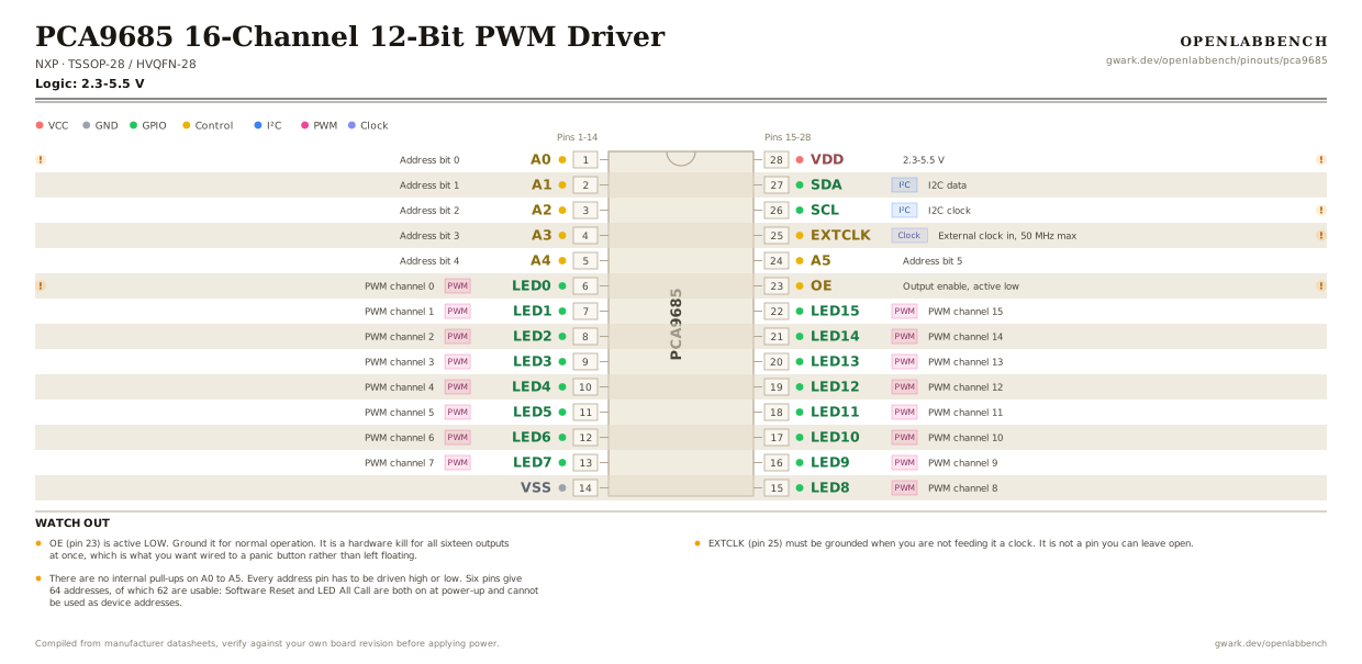
Fig. 1. PCA9685 16-Channel 12-Bit PWM Driver, TSSOP-28. Hover or tap a signal to light up every pin that carries it.
2.Watch out
- OE (pin 23) is active LOW. Ground it for normal operation. It is a hardware kill for all sixteen outputs at once, which is what you want wired to a panic button rather than left floating.
- EXTCLK (pin 25) must be grounded when you are not feeding it a clock. It is not a pin you can leave open.
- There are no internal pull-ups on A0 to A5. Every address pin has to be driven high or low. Six pins give 64 addresses, of which 62 are usable: Software Reset and LED All Call are both on at power-up and cannot be used as device addresses.
- The PWM frequency is global. All sixteen channels share one prescaler, so you cannot run servos at 50 Hz and dim LEDs at 1 kHz from the same chip.
- PRE_SCALE cannot be written unless the SLEEP bit in MODE1 is set. Writes are silently blocked otherwise, which is why so much servo code mysteriously runs at the 200 Hz default. Sleep, set the prescaler, wake, then wait 500 us before clearing RESTART.
- Each channel has a 12-bit ON time and a 12-bit OFF time, not just a duty cycle. Staggering the ON points spreads the current draw across the cycle instead of switching all sixteen at once.
- Outputs are totem pole by default, sinking 25 mA and sourcing 10 mA at 5 V, and can be switched to open drain in software. That is enough for an LED or a servo signal wire, not for a servo's power. On breakout boards the V+ screw terminal is a separate supply for the loads and is not a pin on the chip.
- Frequency range is about 24 Hz to 1526 Hz from the internal 25 MHz oscillator. An external clock up to 50 MHz on EXTCLK raises that and lets several chips share one timebase.
3.Minimum circuit
What has to go around the chip before it will run.
| Part | Between | Why |
|---|---|---|
| 0.1 uF ceramic | VDD (28) to GND | Supply decoupling at the pin. Sixteen outputs switching together is a sharp current step. |
| Enable link | OE (23) to GND | OE is active low, so grounding it enables the outputs. Leaving it floating leaves them undefined. |
| Clock link | EXTCLK (25) to GND | EXTCLK must be grounded when the internal 25 MHz oscillator is used, which is almost always. |
| 4.7 kOhm | SDA (27) to VCC | I2C pull-up on SDA. The bus is open drain and cannot pull itself high. |
| 4.7 kOhm | SCL (26) to VCC | I2C pull-up on SCL. One pair per bus, not per device. |
| Address link | A0 (1) to GND | A0 tied low. No address pin has an internal pull-up, so each one is a wire you have to actually run. |
| Address link | A1 (2) to GND | A1 tied low. Tie it to VDD instead and the address goes up by 2. |
| Address link | A2 (3) to GND | A2 tied low. Tie it to VDD instead and the address goes up by 4. |
| Address link | A3 (4) to GND | A3 tied low. Tie it to VDD instead and the address goes up by 8. |
| Address link | A4 (5) to GND | A4 tied low. Tie it to VDD instead and the address goes up by 16. |
| Address link | A5 (24) to GND | A5 tied low, the most significant bit. All six low puts the chip at 0x40. |
Tie each address pin to VDD instead of ground to move the chip up from 0x40. The load supply is separate: an LED needs its own series resistor, and a servo takes its power from a rail the chip never touches.
4.Full pin reference
Every pin, alias and mapping. This is the table that prints.
Table 2. Pin assignments.
| Pin | Name | Also called | Functions | Notes |
|---|---|---|---|---|
| 1 | A0 | - | Address bit 0 | No internal pull-up. Must be tied high or low. |
| 2 | A1 | - | Address bit 1 | |
| 3 | A2 | - | Address bit 2 | |
| 4 | A3 | - | Address bit 3 | |
| 5 | A4 | - | Address bit 4 | |
| 6 | LED0PWM | - | PWM channel 0 | Totem pole by default: sinks 25 mA, sources 10 mA at 5 V. |
| 7 | LED1PWM | - | PWM channel 1 | |
| 8 | LED2PWM | - | PWM channel 2 | |
| 9 | LED3PWM | - | PWM channel 3 | |
| 10 | LED4PWM | - | PWM channel 4 | |
| 11 | LED5PWM | - | PWM channel 5 | |
| 12 | LED6PWM | - | PWM channel 6 | |
| 13 | LED7PWM | - | PWM channel 7 | |
| 14 | VSS | GND | - | |
| 15 | LED8PWM | - | PWM channel 8 | |
| 16 | LED9PWM | - | PWM channel 9 | |
| 17 | LED10PWM | - | PWM channel 10 | |
| 18 | LED11PWM | - | PWM channel 11 | |
| 19 | LED12PWM | - | PWM channel 12 | |
| 20 | LED13PWM | - | PWM channel 13 | |
| 21 | LED14PWM | - | PWM channel 14 | |
| 22 | LED15PWM | - | PWM channel 15 | |
| 23 | OE | /OE, OE# | Output enable, active low | Low enables all outputs. High disables them in one step, with no I2C transaction. |
| 24 | A5 | - | Address bit 5 | |
| 25 | EXTCLKClock | - | External clock in, 50 MHz max | Ground it when unused. Driving it lets several chips share one timebase. |
| 26 | SCLI²C | - | I2C clock | Fast-mode Plus, to 1 MHz. |
| 27 | SDAI²C | - | I2C data | |
| 28 | VDD2.3-5.5 V | - | - | Powers the chip and sets the output high level. Not the load supply. |
Found a wrong pin? The whole board is one file, data/boards/pca9685.json.