TI / NXP · Integrated circuit
PCF8574 I2C I/O Expander
Eight more pins over two wires, and the chip on every I2C LCD backpack. Quasi-bidirectional outputs, which is the catch.
- Logic level
- 2.5-6 V
- Package
- PDIP-16 / SOIC-16 / TSSOP-16
1.Pinout diagram
Highlight a signalhover to preview, click to keep
Pins 1-8
Pins 9-16
Pin detail
Hover a pin for its mappings and gotchas. Click to keep it here.
- Logic level
- 2.5-6 V
- Package
- PDIP-16 / SOIC-16 / TSSOP-16
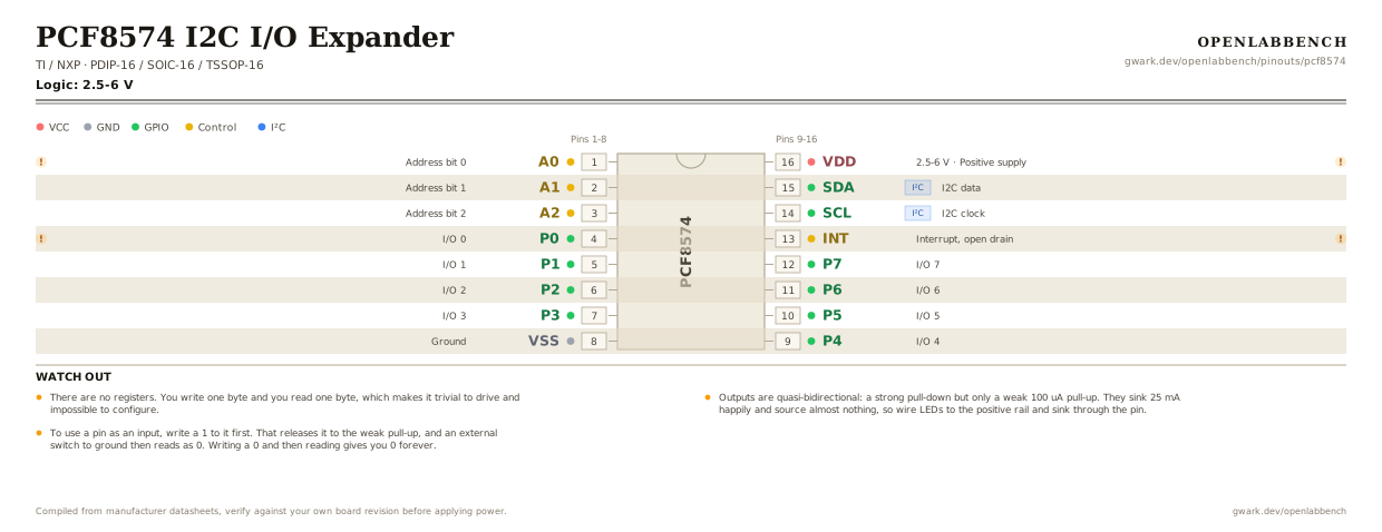
Fig. 1. PCF8574 I2C I/O Expander, PDIP-16. Hover or tap a signal to light up every pin that carries it.
2.Watch out
- There are no registers. You write one byte and you read one byte, which makes it trivial to drive and impossible to configure.
- Outputs are quasi-bidirectional: a strong pull-down but only a weak 100 uA pull-up. They sink 25 mA happily and source almost nothing, so wire LEDs to the positive rail and sink through the pin.
- To use a pin as an input, write a 1 to it first. That releases it to the weak pull-up, and an external switch to ground then reads as 0. Writing a 0 and then reading gives you 0 forever.
- A0, A1 and A2 set the low three address bits: 0x20 to 0x27 on the PCF8574, and 0x38 to 0x3F on the PCF8574A. Sellers mix the two parts freely, so scan the bus before assuming.
- INT (pin 13) is open drain and pulses on any input change, which saves polling. It needs its own pull-up.
- If you need real configurable pull-ups, push-pull outputs or per-pin direction, the MCP23017 does all three for a little more money and a register map.
3.Minimum circuit
What has to go around the chip before it will run.
| Part | Between | Why |
|---|---|---|
| 4.7 kOhm | SDA (15) to VCC | I2C data is open drain and there are no internal pull-ups on the bus. |
| 4.7 kOhm | SCL (14) to VCC | The matching pull-up for the clock line. |
| Wire link | A0 (1) to GND | Address bit 0. These three pins set the I2C address and must not be left floating. |
| Wire link | A1 (2) to GND | Address bit 1. All three low gives 0x20 on the PCF8574, 0x38 on the PCF8574A. |
| Wire link | A2 (3) to GND | Address bit 2. Eight devices fit on one bus, which is the point of the part. |
| 100 nF | VDD (16) to GND | Supply decoupling at the pin. |
| 10 kOhmoptional | INT (13) to VCC | INT is open drain too. Only needed if you use the change interrupt. |
The outputs are quasi-bidirectional: they can only sink 25 mA and source about 100 uA. Drive LEDs to ground, not from the pin, and write a 1 to a pin before using it as an input.
4.Register configuration
Turning a pin on the diagram into a configured pin.
Read and write the port over I2C
Linux i2c-dev
#include <fcntl.h>
#include <unistd.h>
#include <linux/i2c-dev.h>
#include <sys/ioctl.h>

int fd = open("/dev/i2c-1", O_RDWR);
ioctl(fd, I2C_SLAVE, 0x20);        /* A2..A0 all grounded */

uint8_t out = 0x0F;                /* low nibble low, high nibble released */
write(fd, &out, 1);

/* To read a pin you must first write a 1 to it, which releases it
   to the weak pull-up. A pin you last wrote 0 reads 0 forever. */
uint8_t mask = 0xF0;
write(fd, &mask, 1);
uint8_t in;
read(fd, &in, 1);
There are no registers and no direction bits. Writing 1 releases a pin to a weak 100 uA pull-up so it can be read; writing 0 pulls it hard low. Outputs sink 25 mA but barely source, so wire LEDs to the positive rail.
5.Full pin reference
Every pin, alias and mapping. This is the table that prints.
Table 2. Pin assignments.
| Pin | Name | Also called | Functions | Notes |
|---|---|---|---|---|
| 1 | A0 | - | Address bit 0 | Tie high or low. Never leave floating. |
| 2 | A1 | - | Address bit 1 | |
| 3 | A2 | - | Address bit 2 | |
| 4 | P0 | - | I/O 0 | Sinks 25 mA, sources 100 uA. Wire loads to the positive rail. |
| 5 | P1 | - | I/O 1 | |
| 6 | P2 | - | I/O 2 | |
| 7 | P3 | - | I/O 3 | |
| 8 | VSS | GND | Ground | |
| 9 | P4 | - | I/O 4 | |
| 10 | P5 | - | I/O 5 | |
| 11 | P6 | - | I/O 6 | |
| 12 | P7 | - | I/O 7 | |
| 13 | INT | /INT | Interrupt, open drain | Pulses low on any input change. Needs a pull-up. |
| 14 | SCLI²C | - | I2C clock | |
| 15 | SDAI²C | - | I2C data | |
| 16 | VDD2.5-6 V | - | Positive supply | 100 nF to ground at the pin. |
Looking for a substitute?
Primary sources
Found a wrong pin? The whole board is one file, data/boards/pcf8574.json.