Microchip · Microcontroller
PIC16F877A
The PIC that taught a generation of engineering students. 33 I/O, eight ADC channels and a DIP-40 you can still breadboard.
- Logic level
- 2.0-5.5 V
- Package
- PDIP-40 / TQFP-44 / PLCC-44
1.Pinout diagram
Highlight a signalhover to preview, click to keep
Pins 1-20
Pins 21-40
Pin detail
Hover a pin for its mappings and gotchas. Click to keep it here.
- Logic level
- 2.0-5.5 V
- Package
- PDIP-40 / TQFP-44 / PLCC-44
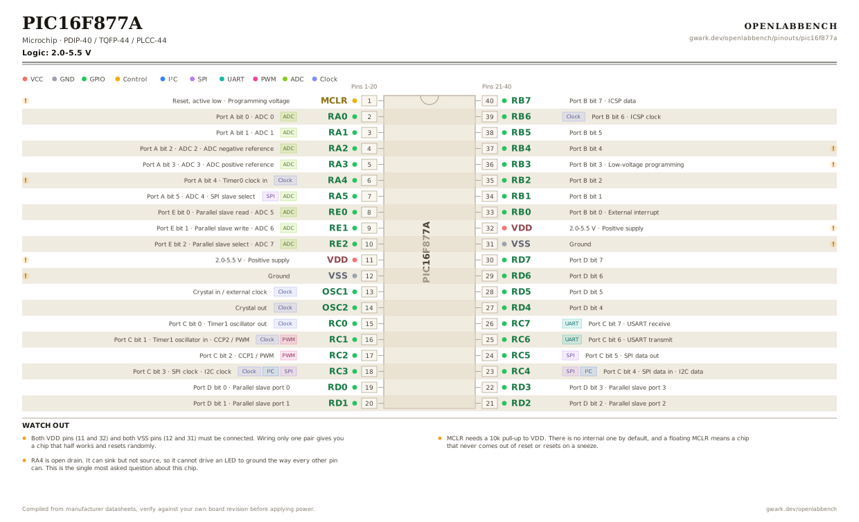
Fig. 1. PIC16F877A, PDIP-40. Hover or tap a signal to light up every pin that carries it.
2.Watch out
- Both VDD pins (11 and 32) and both VSS pins (12 and 31) must be connected. Wiring only one pair gives you a chip that half works and resets randomly.
- MCLR needs a 10k pull-up to VDD. There is no internal one by default, and a floating MCLR means a chip that never comes out of reset or resets on a sneeze.
- RA4 is open drain. It can sink but not source, so it cannot drive an LED to ground the way every other pin can. This is the single most asked question about this chip.
- Port A and Port E default to ANALOG at power-on. Until you write the ADCON1 register, digital reads on those pins return zero. The classic first-project bug.
- RB3 is the low-voltage programming pin. Tie it low if you are not using LVP, or noise can drop the chip into programming mode mid-run.
- RB4 to RB7 have interrupt-on-change, which is how keypads and wake-from-sleep are normally done.
- RB6 and RB7 are the ICSP clock and data. Anything hung on them must not fight the programmer, so keep loads light or add series resistors.
- Superseded for new designs by the PIC16F1939 and the PIC18F family, but still in production and still what a lot of university courses teach.
3.Minimum circuit to run
What has to go around the chip before it will run.
| Part | Between | Why |
|---|---|---|
| 10 kOhm | MCLR (1) to VCC | MCLR is the reset input and has no internal pull-up. Floating, the chip resets at random. |
| 100 nF | VDD (11) to GND | Decoupling at the first supply pair, as close to the pins as the layout allows. |
| 100 nF | VDD (32) to GND | The second VDD pin needs its own. Both pairs must be connected, they are not bonded internally. |
| 20 MHz crystal | OSC1 (13) to OSC2 (14) | There is no internal oscillator on this part. With nothing on OSC1 the chip simply does not run. |
| 22 pF | OSC1 (13) to GND | Crystal load capacitor, 15 to 33 pF depending on the crystal. |
| 22 pF | OSC2 (14) to GND | The matching load capacitor on the other crystal pin. |
The configuration word has to select the oscillator mode as well, HS for 20 MHz. Fitting the crystal is not enough on its own, and the same word is where you turn the watchdog off.
4.Register configuration
Turning a pin on the diagram into a configured pin.
Set up the ports, and stop them being analog
XC8
#include <xc.h>

/* Port A and Port E come up ANALOG. Until this runs, a digital
   read on those pins returns 0 no matter what you wired. */
ADCON1 = 0x06;                 /* PCFG = 0110: all digital */

TRISB  = 0x00;                 /* 0 = output, the opposite of AVR's DDR */
PORTB  = 0xFF;

TRISA  = 0xFF;                 /* 1 = input */
if (PORTAbits.RA0 == 0) {
}

/* RA4 is open drain. It can sink but never source, so an LED
   to ground will not light from this pin. */
TRIS is inverted against AVR's DDR: 0 means output here. And Port A defaults to analog, which is the single most common first-project failure on this chip.
5.Full pin reference
Every pin, alias and mapping. This is the table that prints.
Table 2. Pin assignments.
| Pin | Name | Also called | Functions | Notes |
|---|---|---|---|---|
| 1 | MCLR | VPP, RE3 | Reset, active low, Programming voltage | Needs a 10k pull-up to VDD. Also where 13 V arrives during high-voltage programming. |
| 2 | RA0ADC | AN0 | Port A bit 0, ADC 0 | |
| 3 | RA1ADC | AN1 | Port A bit 1, ADC 1 | |
| 4 | RA2ADC | AN2, VREF- | Port A bit 2, ADC 2, ADC negative reference | |
| 5 | RA3ADC | AN3, VREF+ | Port A bit 3, ADC 3, ADC positive reference | |
| 6 | RA4Clock | T0CKI | Port A bit 4, Timer0 clock in | Open drain only. It cannot source current, so an LED here needs a pull-up, not a series resistor to VDD. |
| 7 | RA5ADCSPI | AN4, SS | Port A bit 5, ADC 4, SPI slave select | |
| 8 | RE0ADC | RD, AN5 | Port E bit 0, Parallel slave read, ADC 5 | |
| 9 | RE1ADC | WR, AN6 | Port E bit 1, Parallel slave write, ADC 6 | |
| 10 | RE2ADC | CS, AN7 | Port E bit 2, Parallel slave select, ADC 7 | |
| 11 | VDD2.0-5.5 V | - | Positive supply | Both VDD pins, 11 and 32, must be connected. |
| 12 | VSS | - | Ground | Both VSS pins, 12 and 31, must be connected. |
| 13 | OSC1Clock | CLKIN | Crystal in / external clock | |
| 14 | OSC2Clock | CLKOUT | Crystal out | |
| 15 | RC0Clock | T1OSO, T1CKI | Port C bit 0, Timer1 oscillator out | |
| 16 | RC1PWMClock | T1OSI, CCP2 | Port C bit 1, Timer1 oscillator in, CCP2 / PWM | |
| 17 | RC2PWM | CCP1 | Port C bit 2, CCP1 / PWM | |
| 18 | RC3SPII²CClock | SCK, SCL | Port C bit 3, SPI clock, I2C clock | |
| 19 | RD0 | PSP0 | Port D bit 0, Parallel slave port 0 | |
| 20 | RD1 | PSP1 | Port D bit 1, Parallel slave port 1 | |
| 21 | RD2 | PSP2 | Port D bit 2, Parallel slave port 2 | |
| 22 | RD3 | PSP3 | Port D bit 3, Parallel slave port 3 | |
| 23 | RC4SPII²C | SDI, SDA | Port C bit 4, SPI data in, I2C data | |
| 24 | RC5SPI | SDO | Port C bit 5, SPI data out | |
| 25 | RC6UART | TX, CK | Port C bit 6, USART transmit | |
| 26 | RC7UART | RX, DT | Port C bit 7, USART receive | |
| 27 | RD4 | PSP4 | Port D bit 4 | |
| 28 | RD5 | PSP5 | Port D bit 5 | |
| 29 | RD6 | PSP6 | Port D bit 6 | |
| 30 | RD7 | PSP7 | Port D bit 7 | |
| 31 | VSS | - | Ground | The second ground. Connect it. |
| 32 | VDD2.0-5.5 V | - | Positive supply | The second supply pin. Connect it. |
| 33 | RB0 | INT | Port B bit 0, External interrupt | |
| 34 | RB1 | - | Port B bit 1 | |
| 35 | RB2 | - | Port B bit 2 | |
| 36 | RB3 | PGM | Port B bit 3, Low-voltage programming | Tie low if you are not using low-voltage programming, or stray noise can put the chip into program mode. |
| 37 | RB4 | - | Port B bit 4 | RB4 to RB7 have interrupt-on-change, the usual way to wake from sleep on a keypad. |
| 38 | RB5 | - | Port B bit 5 | |
| 39 | RB6Clock | PGC | Port B bit 6, ICSP clock | |
| 40 | RB7 | PGD | Port B bit 7, ICSP data |
Primary sources
Found a wrong pin? The whole board is one file, data/boards/pic16f877a.json.