Raspberry Pi · Single-board computer
Raspberry Pi 26-pin GPIO Header
The original Model A and Model B header. Pins 1 to 26 match the 40-pin layout, with three that moved between board revisions.
- Logic level
- 3.3 V
- Package
- 2x13 2.54 mm (P1)
1.Pinout diagram
Highlight a signalhover to preview, click to keep
Odd pins
RPI 26-PIN
Even pins
Pin detail
Hover a pin for its mappings and gotchas. Click to keep it here.
- Logic level
- 3.3 V
- Package
- 2x13 2.54 mm (P1)
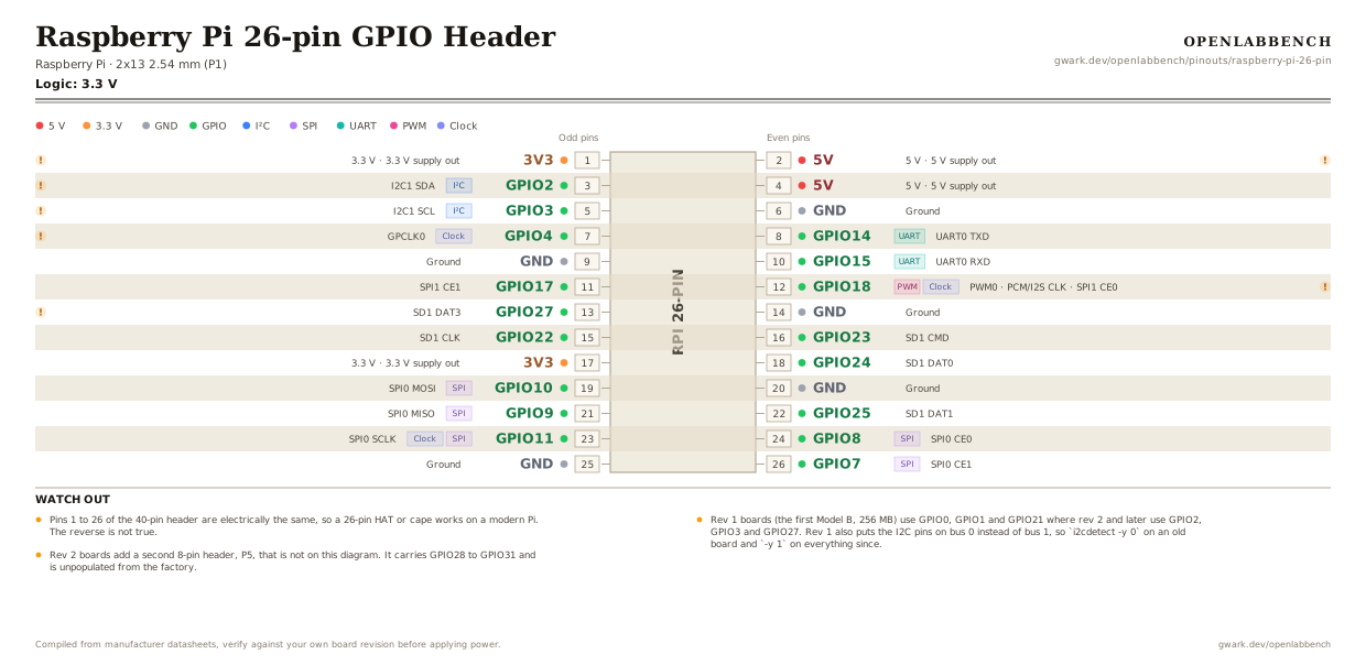
Fig. 1. Raspberry Pi 26-pin GPIO Header, 2x13 2.54 mm (P1). Hover or tap a signal to light up every pin that carries it.
2.Watch out
- Pins 1 to 26 of the 40-pin header are electrically the same, so a 26-pin HAT or cape works on a modern Pi. The reverse is not true.
- Rev 1 boards (the first Model B, 256 MB) use GPIO0, GPIO1 and GPIO21 where rev 2 and later use GPIO2, GPIO3 and GPIO27. Rev 1 also puts the I2C pins on bus 0 instead of bus 1, so `i2cdetect -y 0` on an old board and `-y 1` on everything since.
- Rev 2 boards add a second 8-pin header, P5, that is not on this diagram. It carries GPIO28 to GPIO31 and is unpopulated from the factory.
- 3.3 V only, like every Pi. A 5 V output into any of these damages the SoC.
- GPIO2 and GPIO3 carry fixed 1.8 kOhm pull-ups to 3V3 on the board.
3.Full pin reference
Every pin, alias and mapping. This is the table that prints.
Table 1. Pin assignments.
| Pin | Name | Also called | Functions | Notes |
|---|---|---|---|---|
| 1 | 3V33.3 V | - | 3.3 V supply out | ~50 mA budget shared with pin 17. |
| 2 | 5V5 V | - | 5 V supply out | Fed straight from the USB-C / micro-USB input, upstream of the 3V3 regulator. |
| 3 | GPIO2I²C | BCM 2, SDA1, I2C1 SDA, Rev 1: GPIO0 | I2C1 SDA | Fixed 1.8 kΩ pull-up to 3V3. Rev 1 boards have GPIO0 here, on I2C0 rather than I2C1. |
| 4 | 5V5 V | - | 5 V supply out | |
| 5 | GPIO3I²C | BCM 3, SCL1, I2C1 SCL, Rev 1: GPIO1 | I2C1 SCL | Fixed 1.8 kΩ pull-up to 3V3. Also wakes the Pi from halt when pulled low. Rev 1 boards have GPIO1 here, on I2C0 rather than I2C1. |
| 6 | GND | - | Ground | |
| 7 | GPIO4Clock | BCM 4, GPCLK0 | GPCLK0 | Default 1-Wire bus pin (w1-gpio overlay), used by DS18B20 sensors. |
| 8 | GPIO14UART | BCM 14, TXD0, TXD | UART0 TXD | |
| 9 | GND | - | Ground | |
| 10 | GPIO15UART | BCM 15, RXD0, RXD | UART0 RXD | |
| 11 | GPIO17 | BCM 17 | SPI1 CE1 | |
| 12 | GPIO18PWMClock | BCM 18, PCM_CLK | PWM0, PCM/I2S CLK, SPI1 CE0 | The pin WS2812/NeoPixel libraries use, because it reaches PWM0 via DMA. |
| 13 | GPIO27 | BCM 27, Rev 1: GPIO21 | SD1 DAT3 | Rev 1 boards have GPIO21 here. This is the pin that catches people reusing old code. |
| 14 | GND | - | Ground | |
| 15 | GPIO22 | BCM 22 | SD1 CLK | |
| 16 | GPIO23 | BCM 23 | SD1 CMD | |
| 17 | 3V33.3 V | - | 3.3 V supply out | |
| 18 | GPIO24 | BCM 24 | SD1 DAT0 | |
| 19 | GPIO10SPI | BCM 10, MOSI | SPI0 MOSI | |
| 20 | GND | - | Ground | |
| 21 | GPIO9SPI | BCM 9, MISO | SPI0 MISO | |
| 22 | GPIO25 | BCM 25 | SD1 DAT1 | |
| 23 | GPIO11SPIClock | BCM 11, SCLK | SPI0 SCLK | |
| 24 | GPIO8SPI | BCM 8, CE0 | SPI0 CE0 | |
| 25 | GND | - | Ground | |
| 26 | GPIO7SPI | BCM 7, CE1 | SPI0 CE1 |
Primary sources
Found a wrong pin? The whole board is one file, data/boards/raspberry-pi-26-pin.json.