TI / Nexperia / many · Integrated circuit
74HC00 Quad NAND Gate
Four 2-input NAND gates, the cheapest way to build any logic function at all.
- Logic level
- 2-6 V (HC)
- Package
- PDIP-14 / SOIC-14
1.Pinout diagram
Highlight a signalhover to preview, click to keep
Pins 1-7
74HC00
Pins 8-14
Pin detail
Hover a pin for its mappings and gotchas. Click to keep it here.
- Logic level
- 2-6 V (HC)
- Package
- PDIP-14 / SOIC-14
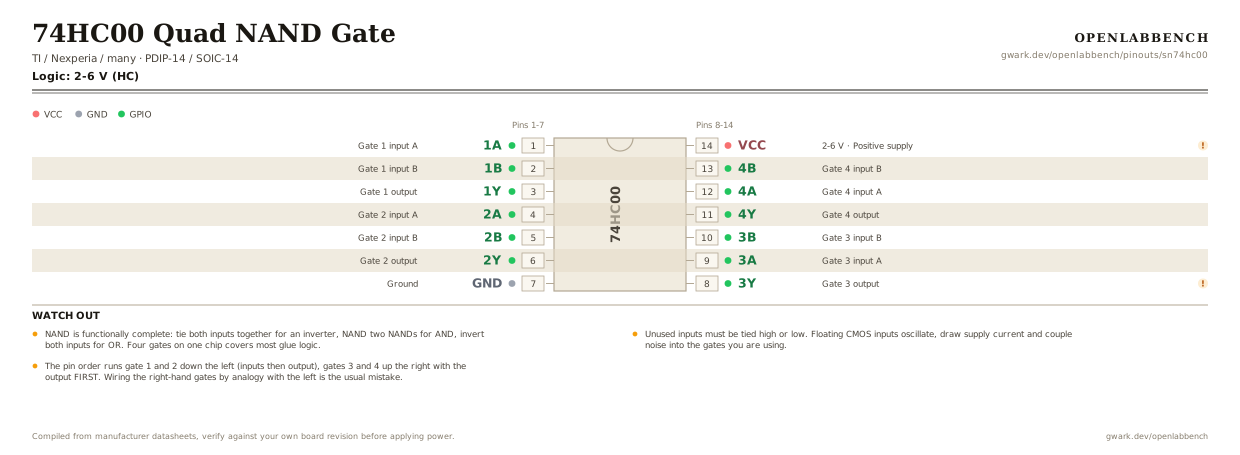
Fig. 1. 74HC00 Quad NAND Gate, PDIP-14. Hover or tap a signal to light up every pin that carries it.
2.Watch out
- NAND is functionally complete: tie both inputs together for an inverter, NAND two NANDs for AND, invert both inputs for OR. Four gates on one chip covers most glue logic.
- Unused inputs must be tied high or low. Floating CMOS inputs oscillate, draw supply current and couple noise into the gates you are using.
- The pin order runs gate 1 and 2 down the left (inputs then output), gates 3 and 4 up the right with the output FIRST. Wiring the right-hand gates by analogy with the left is the usual mistake.
- HC needs an input within about 1 V of its own rail. Driving a 5 V 74HC00 from 3.3 V logic is out of spec; use 74HCT00, which has TTL thresholds.
- Propagation delay is roughly 9 ns at 5 V. For anything slower, the cheaper 74LS00 still exists but draws far more current.
- 100 nF across pins 7 and 14, at the chip. Four gates switching together pull a current spike the supply trace will not like.
3.Set-reset latch
What has to go around the chip before it will run.
| Part | Between | Why |
|---|---|---|
| Wire link | 1Y (3) to 2A (4) | Gate 1 output into gate 2 input. The cross-coupling is what gives the pair memory. |
| Wire link | 2Y (6) to 1B (2) | Gate 2 output back into gate 1. Now each gate holds the other. |
| 10 kOhm | 1A (1) to VCC | Set input, active low. Pull it down to set, and the pull-up keeps it idle high. |
| 10 kOhm | 2B (5) to VCC | Reset input, active low. Taking both inputs low at once is the state the latch has no answer for. |
| 100 nF | VCC (14) to GND | Supply decoupling at the pin. |
Two NAND gates and two resistors debounce a changeover switch perfectly, with no timing constant to tune. It is the oldest trick in the book and still the right one for a SPDT button.
4.Full pin reference
Every pin, alias and mapping. This is the table that prints.
Table 2. Pin assignments.
| Pin | Name | Also called | Functions | Notes |
|---|---|---|---|---|
| 1 | 1A | - | Gate 1 input A | |
| 2 | 1B | - | Gate 1 input B | |
| 3 | 1Y | - | Gate 1 output | |
| 4 | 2A | - | Gate 2 input A | |
| 5 | 2B | - | Gate 2 input B | |
| 6 | 2Y | - | Gate 2 output | |
| 7 | GND | - | Ground | |
| 8 | 3Y | - | Gate 3 output | Output comes first on this side, unlike gates 1 and 2. |
| 9 | 3A | - | Gate 3 input A | |
| 10 | 3B | - | Gate 3 input B | |
| 11 | 4Y | - | Gate 4 output | |
| 12 | 4A | - | Gate 4 input A | |
| 13 | 4B | - | Gate 4 input B | |
| 14 | VCC2-6 V | - | Positive supply | 100 nF to GND at the pin. |
Looking for a substitute?
Primary sources
Found a wrong pin? The whole board is one file, data/boards/sn74hc00.json.