TI / Nexperia / many · Integrated circuit
74HC04 Hex Inverter
Six plain inverters. The cheapest logic chip there is, and the wrong one if your input edge is slow.
- Logic level
- 2-6 V (HC)
- Package
- PDIP-14 / SOIC-14
1.Pinout diagram
Highlight a signalhover to preview, click to keep
Pins 1-7
74HC04
Pins 8-14
Pin detail
Hover a pin for its mappings and gotchas. Click to keep it here.
- Logic level
- 2-6 V (HC)
- Package
- PDIP-14 / SOIC-14
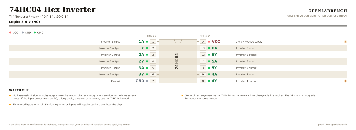
Fig. 1. 74HC04 Hex Inverter, PDIP-14. Hover or tap a signal to light up every pin that carries it.
2.Watch out
- No hysteresis. A slow or noisy edge makes the output chatter through the transition, sometimes several times. If the input comes from an RC, a long cable, a sensor or a switch, use the 74HC14 instead.
- Same pin arrangement as the 74HC14, so the two are interchangeable in a socket. The 14 is a strict upgrade for about the same money.
- Tie unused inputs to a rail. Six floating inverter inputs will happily oscillate and heat the chip.
- Two inverters and an RC make a ring oscillator, but without hysteresis it is jittery. Again, the 74HC14 does this properly.
3.Crystal oscillator
What has to go around the chip before it will run.
| Part | Between | Why |
|---|---|---|
| 1 MOhm | 1A (1) to 1Y (2) | Biases the inverter into its linear region so it amplifies instead of sitting at a rail. |
| Crystal | 1A (1) to 1Y (2) | A fundamental-mode crystal across the same inverter. This is the Pierce oscillator. |
| 22 pF | 1A (1) to GND | Load capacitor on the input side. The crystal's datasheet load, usually 18 to 22 pF. |
| 22 pF | 1Y (2) to GND | The matching load capacitor on the output side. |
| 100 nF | VCC (14) to GND | Supply decoupling at the pin. |
Buffer the output with a second inverter before you use it anywhere, so loading the oscillator does not pull it off frequency. An HCU04, the unbuffered version, oscillates more reliably here than the HC04.
4.Full pin reference
Every pin, alias and mapping. This is the table that prints.
Table 2. Pin assignments.
| Pin | Name | Also called | Functions | Notes |
|---|---|---|---|---|
| 1 | 1A | - | Inverter 1 input | |
| 2 | 1Y | - | Inverter 1 output | |
| 3 | 2A | - | Inverter 2 input | |
| 4 | 2Y | - | Inverter 2 output | |
| 5 | 3A | - | Inverter 3 input | |
| 6 | 3Y | - | Inverter 3 output | |
| 7 | GND | - | Ground | |
| 8 | 4Y | - | Inverter 4 output | Output first on this side. |
| 9 | 4A | - | Inverter 4 input | |
| 10 | 5Y | - | Inverter 5 output | |
| 11 | 5A | - | Inverter 5 input | |
| 12 | 6Y | - | Inverter 6 output | |
| 13 | 6A | - | Inverter 6 input | |
| 14 | VCC2-6 V | - | Positive supply | 100 nF at the pin. |
Looking for a substitute?
Primary sources
Found a wrong pin? The whole board is one file, data/boards/sn74hc04.json.