TI / Nexperia / many · Integrated circuit
74HC138 3-to-8 Decoder
Three address lines in, one of eight outputs low. The standard way to generate chip selects in a homebrew computer.
- Logic level
- 2-6 V (HC)
- Package
- PDIP-16 / SOIC-16
1.Pinout diagram
Highlight a signalhover to preview, click to keep
Pins 1-8
Pins 9-16
Pin detail
Hover a pin for its mappings and gotchas. Click to keep it here.
- Logic level
- 2-6 V (HC)
- Package
- PDIP-16 / SOIC-16
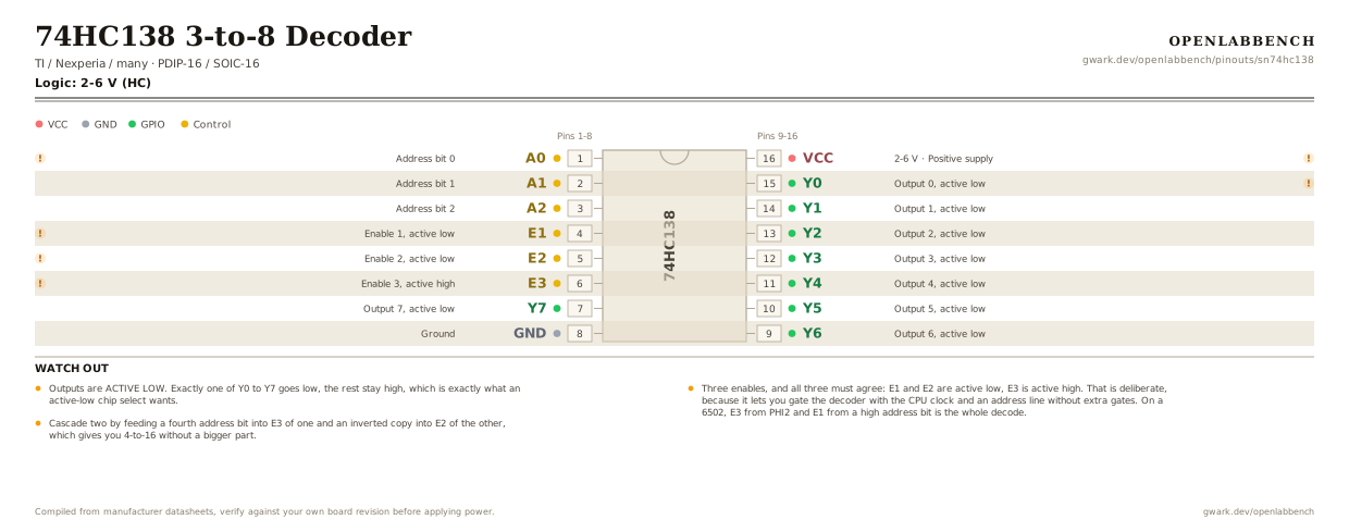
Fig. 1. 74HC138 3-to-8 Decoder, PDIP-16. Hover or tap a signal to light up every pin that carries it.
2.Watch out
- Outputs are ACTIVE LOW. Exactly one of Y0 to Y7 goes low, the rest stay high, which is exactly what an active-low chip select wants.
- Three enables, and all three must agree: E1 and E2 are active low, E3 is active high. That is deliberate, because it lets you gate the decoder with the CPU clock and an address line without extra gates. On a 6502, E3 from PHI2 and E1 from a high address bit is the whole decode.
- Cascade two by feeding a fourth address bit into E3 of one and an inverted copy into E2 of the other, which gives you 4-to-16 without a bigger part.
- Leaving any enable floating means the decoder either never fires or fires constantly. This is the usual reason a breadboard bus has two devices driving at once.
- For 4-to-16 in one package the 74HC154 does it directly, at 24 pins.
3.Minimum circuit
What has to go around the chip before it will run.
| Part | Between | Why |
|---|---|---|
| Wire link | E1 (4) to GND | Enable 1 is active low. Any enable left floating and all eight outputs stay high. |
| Wire link | E2 (5) to GND | Enable 2, also active low. |
| Wire link | E3 (6) to VCC | Enable 3 is the active high one. All three have to agree before an output goes low. |
| 100 nF | VCC (16) to GND | Supply decoupling at the pin. |
The outputs are active low: the selected one goes low and the other seven stay high. Feed a real address line into an enable rather than tying it, and the decoder does the chip selecting for a whole bus.
4.Full pin reference
Every pin, alias and mapping. This is the table that prints.
Table 2. Pin assignments.
| Pin | Name | Also called | Functions | Notes |
|---|---|---|---|---|
| 1 | A0 | A | Address bit 0 | Low bit of the output number. |
| 2 | A1 | B | Address bit 1 | |
| 3 | A2 | C | Address bit 2 | |
| 4 | E1 | /G2A | Enable 1, active low | Must be low. All three enables must agree or nothing happens. |
| 5 | E2 | /G2B | Enable 2, active low | Must be low. |
| 6 | E3 | G1 | Enable 3, active high | Must be high. Drive from PHI2 to qualify the decode with the bus cycle. |
| 7 | Y7 | - | Output 7, active low | |
| 8 | GND | - | Ground | |
| 9 | Y6 | - | Output 6, active low | |
| 10 | Y5 | - | Output 5, active low | |
| 11 | Y4 | - | Output 4, active low | |
| 12 | Y3 | - | Output 3, active low | |
| 13 | Y2 | - | Output 2, active low | |
| 14 | Y1 | - | Output 1, active low | |
| 15 | Y0 | - | Output 0, active low | Selected when A2, A1 and A0 are all low. |
| 16 | VCC2-6 V | - | Positive supply | 100 nF at the pin. |
Looking for a substitute?
Primary sources
Found a wrong pin? The whole board is one file, data/boards/sn74hc138.json.