TI / Nexperia / many · Integrated circuit
74HC14 Hex Schmitt Inverter
Six inverters with hysteresis. The part that turns a mushy signal into a clean edge, debounces a switch with one resistor and one cap, and makes an oscillator out of nothing.
- Logic level
- 2-6 V (HC)
- Package
- PDIP-14 / SOIC-14
1.Pinout diagram
Highlight a signalhover to preview, click to keep
Pins 1-7
Pins 8-14
Pin detail
Hover a pin for its mappings and gotchas. Click to keep it here.
- Logic level
- 2-6 V (HC)
- Package
- PDIP-14 / SOIC-14
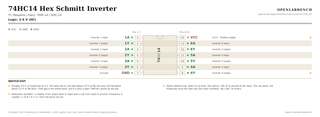
Fig. 1. 74HC14 Hex Schmitt Inverter, PDIP-14. Hover or tap a signal to light up every pin that carries it.
2.Watch out
- Roughly 0.9 V of hysteresis at 5 V: the input has to rise past about 2.9 V to flip one way and fall below about 2.0 V to flip back. That gap is the whole point, and it is why a plain 74HC04 cannot do this job.
- Switch debouncing: switch to ground, 10k pull-up, 100 nF to ground at the input. The cap slews, the hysteresis turns the slew into one clean transition. No code, no timers.
- Relaxation oscillator: a resistor from output back to input and a cap from input to ground. Frequency is roughly 1 / (0.8 x R x C). One chip gives you six.
- It also rescues slow edges from long cables, opto-couplers and photodiodes, all of which produce ramps a normal logic input will chatter on.
- Pin order alternates input then output down the left, and output then input up the right, the same as the 74HC00.
- The CD40106 is the same function in 4000-series CMOS, which runs to 18 V and is handy when the signal swings above 6 V.
3.Relaxation oscillator
What has to go around the chip before it will run.
| Part | Between | Why |
|---|---|---|
| 100 kOhm | 1Y (2) to 1A (1) | Feeds the output back to the input. The capacitor charges through it until the threshold flips the gate. |
| 100 nF | 1A (1) to GND | Sets the period with the resistor, roughly 0.8 x R x C on an HC14. |
| 100 nF | VCC (14) to GND | Supply decoupling at the pin. |
Only a Schmitt input does this. The same two parts on a plain 74HC04 produce a sine-ish mess or nothing at all, because there is no hysteresis to snap the transition.
4.Full pin reference
Every pin, alias and mapping. This is the table that prints.
Table 2. Pin assignments.
| Pin | Name | Also called | Functions | Notes |
|---|---|---|---|---|
| 1 | 1A | - | Inverter 1 input | |
| 2 | 1Y | - | Inverter 1 output | |
| 3 | 2A | - | Inverter 2 input | |
| 4 | 2Y | - | Inverter 2 output | |
| 5 | 3A | - | Inverter 3 input | |
| 6 | 3Y | - | Inverter 3 output | |
| 7 | GND | - | Ground | |
| 8 | 4Y | - | Inverter 4 output | Output first on this side, unlike inverters 1 to 3. |
| 9 | 4A | - | Inverter 4 input | |
| 10 | 5Y | - | Inverter 5 output | |
| 11 | 5A | - | Inverter 5 input | |
| 12 | 6Y | - | Inverter 6 output | |
| 13 | 6A | - | Inverter 6 input | |
| 14 | VCC2-6 V | - | Positive supply | Tie unused inputs to a rail. 100 nF at the pin. |
Looking for a substitute?
Primary sources
Found a wrong pin? The whole board is one file, data/boards/sn74hc14.json.