TI / Nexperia / many · Integrated circuit
74HC165 Shift Register (parallel in)
Eight inputs into three microcontroller pins. The mirror image of the 74HC595, and the part you want for a bank of buttons.
- Logic level
- 2-6 V (HC)
- Package
- PDIP-16 / SOIC-16
1.Pinout diagram
Highlight a signalhover to preview, click to keep
Pins 1-8
74HC165
Pins 9-16
Pin detail
Hover a pin for its mappings and gotchas. Click to keep it here.
- Logic level
- 2-6 V (HC)
- Package
- PDIP-16 / SOIC-16
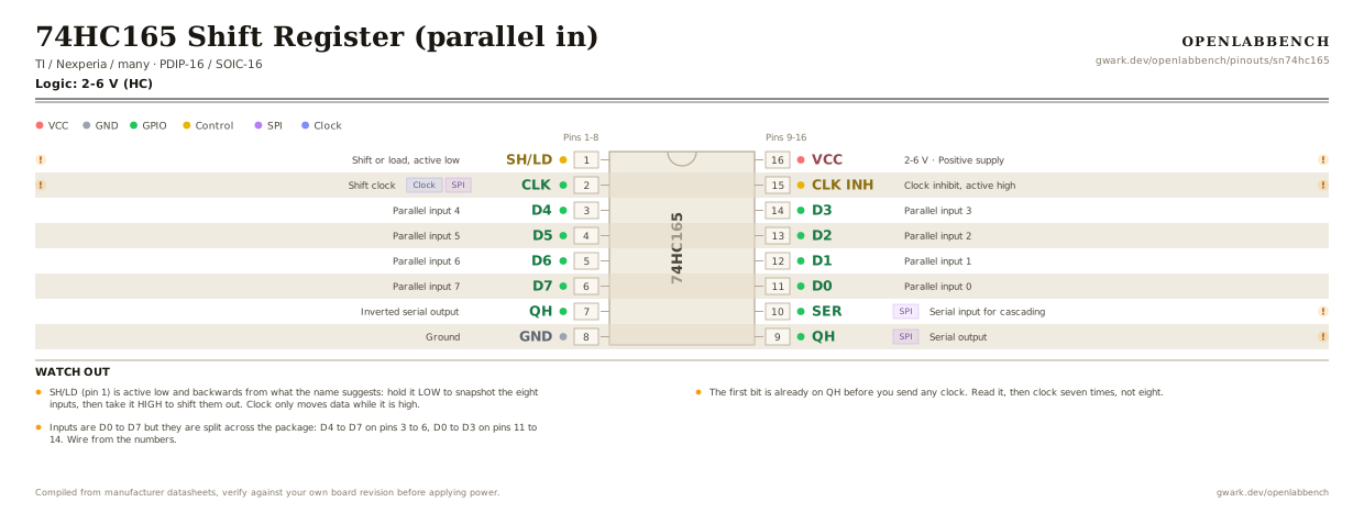
Fig. 1. 74HC165 Shift Register (parallel in), PDIP-16. Hover or tap a signal to light up every pin that carries it.
2.Watch out
- SH/LD (pin 1) is active low and backwards from what the name suggests: hold it LOW to snapshot the eight inputs, then take it HIGH to shift them out. Clock only moves data while it is high.
- The first bit is already on QH before you send any clock. Read it, then clock seven times, not eight.
- Inputs are D0 to D7 but they are split across the package: D4 to D7 on pins 3 to 6, D0 to D3 on pins 11 to 14. Wire from the numbers.
- Chain by feeding QH of one chip into SER (pin 10) of the next, and share SH/LD and CLK. Read the far chip first.
- CLK INH (pin 15) gates the clock. Ground it unless you need it, or the register will not shift.
- Inputs have no internal pull-ups. A bank of buttons needs a resistor per input, which is the one place the PCF8574 is less work.
3.Minimum circuit
What has to go around the chip before it will run.
| Part | Between | Why |
|---|---|---|
| Wire link | CLK INH (15) to GND | Clock inhibit is active high. Tied low the register clocks normally. |
| Wire link | SER (10) to GND | Serial input of the first stage. Tie it, or chain it from the previous chip's QH. |
| 100 nF | VCC (16) to GND | Supply decoupling at the pin. |
Pulse SH/LD (1) low to latch the eight inputs, then clock them out most significant first. Holding it low keeps loading and you read the same pin eight times.
4.Full pin reference
Every pin, alias and mapping. This is the table that prints.
Table 2. Pin assignments.
| Pin | Name | Also called | Functions | Notes |
|---|---|---|---|---|
| 1 | SH/LD | PL, LOAD | Shift or load, active low | Low snapshots the inputs, high lets the clock shift them out. |
| 2 | CLKSPIClock | CP | Shift clock | This is SCK. |
| 3 | D4 | - | Parallel input 4 | |
| 4 | D5 | - | Parallel input 5 | |
| 5 | D6 | - | Parallel input 6 | |
| 6 | D7 | - | Parallel input 7 | |
| 7 | QH | /Q7, QH bar | Inverted serial output | |
| 8 | GND | - | Ground | |
| 9 | QHSPI | Q7, SO | Serial output | This is MISO. The first bit is here before the first clock. |
| 10 | SERSPI | DS, SI | Serial input for cascading | Feed the previous chip's QH in here. Tie low on a single chip. |
| 11 | D0 | - | Parallel input 0 | |
| 12 | D1 | - | Parallel input 1 | |
| 13 | D2 | - | Parallel input 2 | |
| 14 | D3 | - | Parallel input 3 | |
| 15 | CLK INH | CE | Clock inhibit, active high | Ground it. High here blocks the clock entirely. |
| 16 | VCC2-6 V | - | Positive supply | 100 nF to GND at the pin. |
Looking for a substitute?
Primary sources
Found a wrong pin? The whole board is one file, data/boards/sn74hc165.json.