TI / Nexperia / many · Integrated circuit
74HC245 Octal Bus Transceiver
Eight bidirectional buffers with a direction pin and a tri-state enable. What you put between a CPU bus and anything you do not fully trust.
- Logic level
- 2-6 V (HC)
- Package
- PDIP-20 / SOIC-20
1.Pinout diagram
Highlight a signalhover to preview, click to keep
Pins 1-10
Pins 11-20
Pin detail
Hover a pin for its mappings and gotchas. Click to keep it here.
- Logic level
- 2-6 V (HC)
- Package
- PDIP-20 / SOIC-20
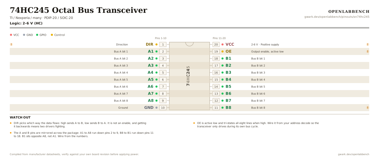
Fig. 1. 74HC245 Octal Bus Transceiver, PDIP-20. Hover or tap a signal to light up every pin that carries it.
2.Watch out
- DIR picks which way the data flows: high sends A to B, low sends B to A. It is not an enable, and getting it backwards means two drivers fighting.
- OE is active low and tri-states all eight lines when high. Wire it from your address decode so the transceiver only drives during its own bus cycle.
- The A and B pins are mirrored across the package: A1 to A8 run down pins 2 to 9, B8 to B1 run down pins 11 to 18. B1 sits opposite A8, not A1. Wire from the numbers.
- Each output drives about 6 mA, far more than a microcontroller pin, which is the point when a bus has to reach across a backplane or a ribbon cable.
- It does not level shift on its own: A and B share one supply. For a genuine level translation use a 74LVC245 powered at the lower rail, which is 5 V tolerant on its inputs.
- Commonly used simply as a strong output buffer with DIR tied high and OE grounded.
3.Minimum circuit
What has to go around the chip before it will run.
| Part | Between | Why |
|---|---|---|
| Wire link | OE (19) to GND | Output enable is active low. Left floating the buffer stays in high impedance and looks like a dead chip. |
| Wire link | DIR (1) to VCC | Direction high sends A to B. Drive this pin instead if the bus has to turn around. |
| 100 nF | VCC (20) to GND | Supply decoupling at the pin, and it matters here: eight outputs can switch at once. |
Both sides are driven outputs when enabled, so never tie DIR by accident on a shared bus: two buffers pointing at each other is a short between whatever is driving them.
4.Full pin reference
Every pin, alias and mapping. This is the table that prints.
Table 2. Pin assignments.
| Pin | Name | Also called | Functions | Notes |
|---|---|---|---|---|
| 1 | DIR | - | Direction | High: A drives B. Low: B drives A. |
| 2 | A1 | - | Bus A bit 1 | |
| 3 | A2 | - | Bus A bit 2 | |
| 4 | A3 | - | Bus A bit 3 | |
| 5 | A4 | - | Bus A bit 4 | |
| 6 | A5 | - | Bus A bit 5 | |
| 7 | A6 | - | Bus A bit 6 | |
| 8 | A7 | - | Bus A bit 7 | |
| 9 | A8 | - | Bus A bit 8 | |
| 10 | GND | - | Ground | |
| 11 | B8 | - | Bus B bit 8 | B8 sits opposite A1, not A8. The two buses run in opposite directions across the package. |
| 12 | B7 | - | Bus B bit 7 | |
| 13 | B6 | - | Bus B bit 6 | |
| 14 | B5 | - | Bus B bit 5 | |
| 15 | B4 | - | Bus B bit 4 | |
| 16 | B3 | - | Bus B bit 3 | |
| 17 | B2 | - | Bus B bit 2 | |
| 18 | B1 | - | Bus B bit 1 | |
| 19 | OE | /OE, /G | Output enable, active low | Ground to drive. High tri-states all eight lines. |
| 20 | VCC2-6 V | - | Positive supply | 100 nF at the pin. Eight lines switching at once is a real current spike. |
Looking for a substitute?
Primary sources
Found a wrong pin? The whole board is one file, data/boards/sn74hc245.json.