TI / Nexperia / many · Integrated circuit
74HC4067 16-Channel Analog Multiplexer
Turns one ADC pin into sixteen. An analog switch, not a buffer, so it passes signals both ways and brings its own resistance along.
- Logic level
- 2-6 V
- Package
- PDIP-24 / SOIC-24 / SSOP-24
1.Pinout diagram
Highlight a signalhover to preview, click to keep
Pins 1-12
Pins 13-24
Pin detail
Hover a pin for its mappings and gotchas. Click to keep it here.
- Logic level
- 2-6 V
- Package
- PDIP-24 / SOIC-24 / SSOP-24
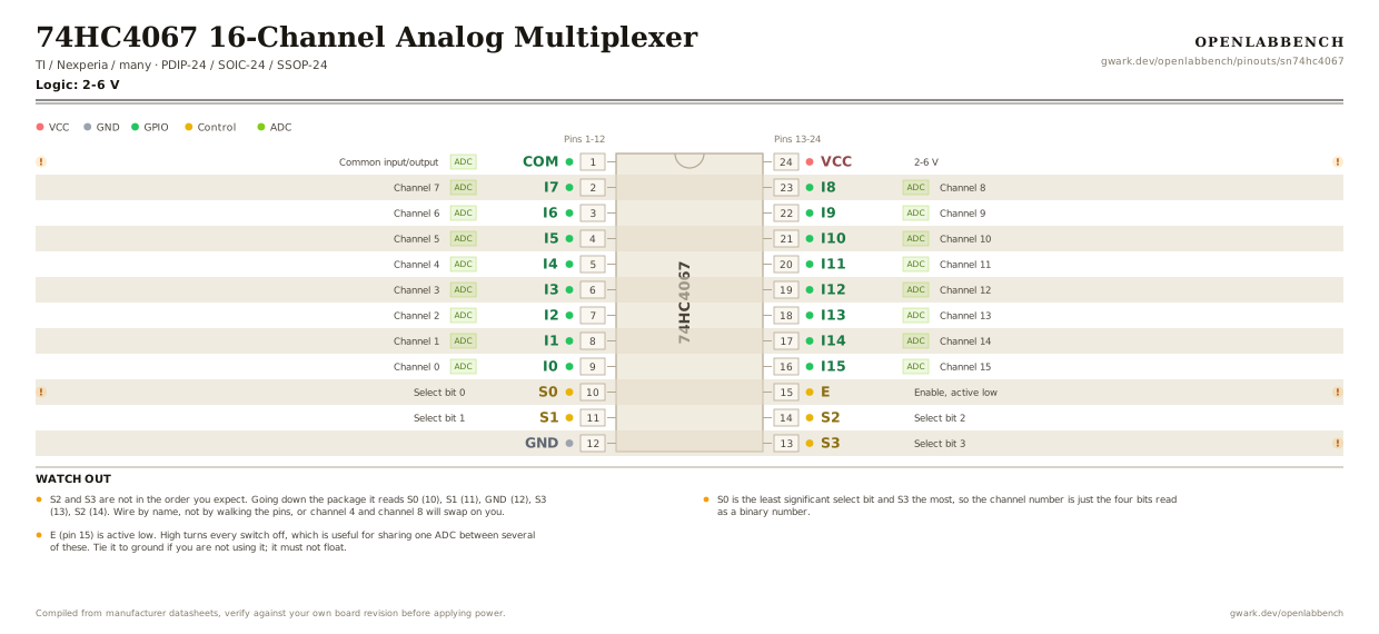
Fig. 1. 74HC4067 16-Channel Analog Multiplexer, PDIP-24. Hover or tap a signal to light up every pin that carries it.
2.Watch out
- S2 and S3 are not in the order you expect. Going down the package it reads S0 (10), S1 (11), GND (12), S3 (13), S2 (14). Wire by name, not by walking the pins, or channel 4 and channel 8 will swap on you.
- S0 is the least significant select bit and S3 the most, so the channel number is just the four bits read as a binary number.
- E (pin 15) is active low. High turns every switch off, which is useful for sharing one ADC between several of these. Tie it to ground if you are not using it; it must not float.
- This is a switch, not an amplifier. The signal has to stay between GND and VCC, so it cannot pass a waveform that swings negative without biasing it first.
- On resistance is about 80 ohms at 6 V and 90 at 4.5 V, up to 180 at worst case, and it changes with the signal level. Into a high-impedance ADC that does not matter; driving anything that draws current, it is a divider you did not design.
- After switching channels, give the ADC time. The sample capacitor has to charge through that on resistance, and reading immediately gives you a blend of the last channel and this one.
- It is bidirectional, so the same part is a 1-to-16 demultiplexer with the signal going the other way. The CD4051 is the 8-channel version of the same idea.
3.Minimum circuit as a 16-input expander
What has to go around the chip before it will run.
| Part | Between | Why |
|---|---|---|
| 0.1 uF ceramic | VCC (24) to GND | Supply decoupling at the pin. Switching all sixteen channels pulls charge out of the rail in steps. |
| Enable link | E (15) to GND | E is active low, so grounding it keeps the selected switch on. Floating leaves the whole chip in an undefined state. |
| To the ADC | COM (1) to MCU | The common pin is the one analog input all sixteen channels share. S0 to S3 pick which one reaches it. |
S0 to S3 go to four ordinary GPIOs. Nothing else is needed: the channels connect straight to whatever you are measuring, as long as it sits between GND and VCC.
4.Full pin reference
Every pin, alias and mapping. This is the table that prints.
Table 2. Pin assignments.
| Pin | Name | Also called | Functions | Notes |
|---|---|---|---|---|
| 1 | COMADC | COMMON, SIG, Z | Common input/output | The shared end. To your ADC pin when multiplexing in, from your source when demultiplexing out. |
| 2 | I7ADC | - | Channel 7 | |
| 3 | I6ADC | - | Channel 6 | |
| 4 | I5ADC | - | Channel 5 | |
| 5 | I4ADC | - | Channel 4 | |
| 6 | I3ADC | - | Channel 3 | |
| 7 | I2ADC | - | Channel 2 | |
| 8 | I1ADC | - | Channel 1 | |
| 9 | I0ADC | - | Channel 0 | |
| 10 | S0 | A | Select bit 0 | Least significant bit of the channel number. |
| 11 | S1 | B | Select bit 1 | |
| 12 | GND | - | - | |
| 13 | S3 | D | Select bit 3 | Most significant bit, and it comes before S2 in the package. This is the pin people miswire. |
| 14 | S2 | C | Select bit 2 | |
| 15 | E | EN, INH | Enable, active low | Low enables. High disconnects all sixteen channels. |
| 16 | I15ADC | - | Channel 15 | |
| 17 | I14ADC | - | Channel 14 | |
| 18 | I13ADC | - | Channel 13 | |
| 19 | I12ADC | - | Channel 12 | |
| 20 | I11ADC | - | Channel 11 | |
| 21 | I10ADC | - | Channel 10 | |
| 22 | I9ADC | - | Channel 9 | |
| 23 | I8ADC | - | Channel 8 | |
| 24 | VCC2-6 V | - | - | Also the upper limit on any signal passing through the switches. |
Primary sources
Found a wrong pin? The whole board is one file, data/boards/sn74hc4067.json.