Texas Instruments / Nexperia / many · Integrated circuit
74HC595 Shift Register
8-bit serial-in, parallel-out shift register with a separate output latch. Three microcontroller pins buy you eight outputs, and chaining Q7S into the next chip's DS extends that indefinitely.
- Logic level
- 2-6 V (HC)
- Package
- PDIP-16 / SOIC-16 / TSSOP-16
1.Pinout diagram
Highlight a signalhover to preview, click to keep
Pins 1-8
Pins 9-16
Pin detail
Hover a pin for its mappings and gotchas. Click to keep it here.
- Logic level
- 2-6 V (HC)
- Package
- PDIP-16 / SOIC-16 / TSSOP-16
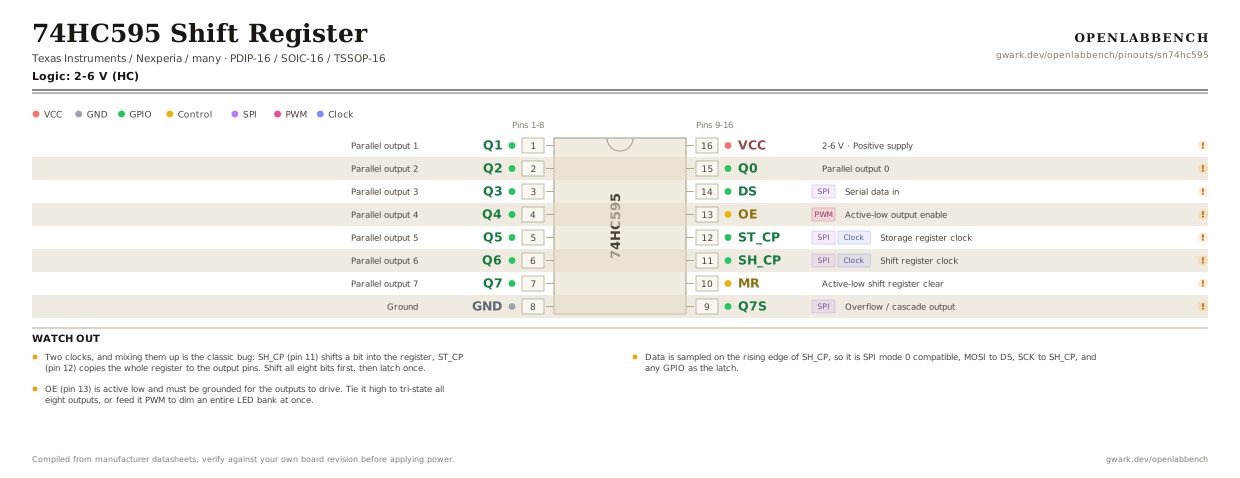
Fig. 1. 74HC595 Shift Register, PDIP-16. Hover or tap a signal to light up every pin that carries it.
2.Watch out
- Two clocks, and mixing them up is the classic bug: SH_CP (pin 11) shifts a bit into the register, ST_CP (pin 12) copies the whole register to the output pins. Shift all eight bits first, then latch once.
- Data is sampled on the rising edge of SH_CP, so it is SPI mode 0 compatible, MOSI to DS, SCK to SH_CP, and any GPIO as the latch.
- OE (pin 13) is active low and must be grounded for the outputs to drive. Tie it high to tri-state all eight outputs, or feed it PWM to dim an entire LED bank at once.
- MR (pin 10) is active low and must be tied to VCC for normal operation. It clears the shift register but not the output latch.
- Output current is around 6 mA per pin and 70 mA for the whole package. For LED matrices or relays use the TPIC6B595, which has 150 mA open-drain sinks.
- Q0 is pin 15, on the far side from Q1-Q7. The output order on the package is not the order you would draw it.
- HC inputs need a level near their own supply rail. A 5 V 74HC595 clocked from 3.3 V logic will drop bits, use the 74HCT595, which has TTL input thresholds, or run the register at 3.3 V.
3.Minimum circuit
What has to go around the chip before it will run.
| Part | Between | Why |
|---|---|---|
| 100 nF | VCC (16) to GND | Eight outputs switching together is a real current step. |
| Wire link | OE (13) to GND | Active low output enable. Left floating the outputs stay tri-stated and nothing lights. |
| Wire link | MR (10) to VCC | Active low clear. Left floating the register clears at random. |
OE can take a PWM signal instead of a ground link, which dims every output at once.
4.Register configuration
Turning a pin on the diagram into a configured pin.
Shift out a byte over SPI
avr-libc
#include <avr/io.h>

/* The 595 is SPI mode 0. MOSI to DS, SCK to SH_CP, any GPIO to ST_CP. */
DDRB |= (1 << PB3) | (1 << PB5) | (1 << PB2);   /* MOSI, SCK, latch */
SPCR  = (1 << SPE) | (1 << MSTR);               /* enable, 1/4 clock */

void shift_out(uint8_t v) {
    SPDR = v;
    while (!(SPSR & (1 << SPIF))) { }           /* wait for the byte */
    PORTB |=  (1 << PB2);                       /* latch rising edge */
    PORTB &= ~(1 << PB2);
}
Two clocks, and swapping them is the classic bug. SH_CP shifts one bit in; ST_CP copies the whole register to the output pins. Shift all eight bits first, then latch once.
5.Full pin reference
Every pin, alias and mapping. This is the table that prints.
Table 2. Pin assignments.
| Pin | Name | Also called | Functions | Notes |
|---|---|---|---|---|
| 1 | Q1 | QB | Parallel output 1 | |
| 2 | Q2 | QC | Parallel output 2 | |
| 3 | Q3 | QD | Parallel output 3 | |
| 4 | Q4 | QE | Parallel output 4 | |
| 5 | Q5 | QF | Parallel output 5 | |
| 6 | Q6 | QG | Parallel output 6 | |
| 7 | Q7 | QH | Parallel output 7 | |
| 8 | GND | - | Ground | |
| 9 | Q7SSPI | QH', SQH, Serial out | Overflow / cascade output | Wire to the next chip's DS to chain registers. One clock behind the latch. |
| 10 | MR | SRCLR, /MR | Active-low shift register clear | Tie to VCC for normal use. Clears the shift register only, the latch keeps its value until ST_CP. |
| 11 | SH_CPSPIClock | SRCLK, SCK, CLOCK | Shift register clock | Rising edge shifts DS into the register. This is SCK. |
| 12 | ST_CPSPIClock | RCLK, LATCH | Storage register clock | Rising edge copies the shift register to Q0-Q7. This is the latch pin. |
| 13 | OEPWM | /OE, G, ENABLE | Active-low output enable | Ground it to enable outputs. PWM here dims every output together. |
| 14 | DSSPI | SER, SI, DATA, A | Serial data in | This is MOSI. |
| 15 | Q0 | QA | Parallel output 0 | First bit out, but physically opposite Q1-Q7. |
| 16 | VCC2-6 V | - | Positive supply | 100 nF decoupling at the pin; shift registers switch eight outputs at once. |
Looking for a substitute?
Primary sources
Found a wrong pin? The whole board is one file, data/boards/sn74hc595.json.