TI / Nexperia / many · Integrated circuit
74HC74 Dual D Flip-Flop
Two edge-triggered D flip-flops with preset and clear. One bit of memory, a divide-by-two, or a proper synchronizer for an async input.
- Logic level
- 2-6 V (HC)
- Package
- PDIP-14 / SOIC-14
1.Pinout diagram
Highlight a signalhover to preview, click to keep
Pins 1-7
Pins 8-14
Pin detail
Hover a pin for its mappings and gotchas. Click to keep it here.
- Logic level
- 2-6 V (HC)
- Package
- PDIP-14 / SOIC-14
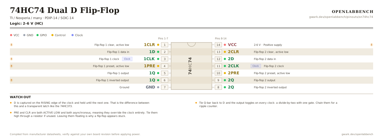
Fig. 1. 74HC74 Dual D Flip-Flop, PDIP-14. Hover or tap a signal to light up every pin that carries it.
2.Watch out
- D is captured on the RISING edge of the clock and held until the next one. That is the difference between this and a transparent latch like the 74HC373.
- Tie Q-bar back to D and the output toggles on every clock: a divide-by-two with one gate. Chain them for a ripple counter.
- PRE and CLR are both ACTIVE LOW and both asynchronous, meaning they override the clock entirely. Tie them high through a resistor if unused. Leaving them floating is why a flip-flop appears stuck.
- Asserting PRE and CLR together is an illegal state: both outputs go high and the next release is a race. Never drive them from the same logic without interlocking.
- This is the right part for bringing an asynchronous signal into a clocked system. Two in series, clocked by your system clock, resolves metastability to a vanishing probability.
- Setup time is about 15 ns at 5 V. Data must be stable that long before the clock edge or the output is undefined.
3.Divide by two
What has to go around the chip before it will run.
| Part | Between | Why |
|---|---|---|
| Wire link | 1Q (6) to 1D (2) | Inverted output back to D. Every clock edge flips the state, so the output runs at half the clock. |
| Wire link | 1PRE (4) to VCC | Preset is active low and has no internal pull-up. Floating, the flip-flop sets itself at random. |
| Wire link | 1CLR (1) to VCC | Clear is active low as well. Both have to be held high for the flip-flop to clock at all. |
| 100 nF | VCC (14) to GND | Supply decoupling at the pin. |
Chain the second flip-flop onto the first for divide by four. The output is also a clean 50 percent duty cycle whatever the input looked like, which is the other reason to do this.
4.Full pin reference
Every pin, alias and mapping. This is the table that prints.
Table 2. Pin assignments.
| Pin | Name | Also called | Functions | Notes |
|---|---|---|---|---|
| 1 | 1CLR | /1CLR, 1RESET | Flip-flop 1 clear, active low | Asynchronous. Tie high if unused. |
| 2 | 1D | - | Flip-flop 1 data in | |
| 3 | 1CLKClock | - | Flip-flop 1 clock | Captures D on the rising edge. |
| 4 | 1PRE | /1PRE, 1SET | Flip-flop 1 preset, active low | Asynchronous. Tie high if unused. |
| 5 | 1Q | - | Flip-flop 1 output | |
| 6 | 1Q | /1Q, 1Q bar | Flip-flop 1 inverted output | Tie this back to 1D for a divide-by-two. |
| 7 | GND | - | Ground | |
| 8 | 2Q | /2Q, 2Q bar | Flip-flop 2 inverted output | |
| 9 | 2Q | - | Flip-flop 2 output | |
| 10 | 2PRE | /2PRE | Flip-flop 2 preset, active low | |
| 11 | 2CLKClock | - | Flip-flop 2 clock | |
| 12 | 2D | - | Flip-flop 2 data in | |
| 13 | 2CLR | /2CLR | Flip-flop 2 clear, active low | |
| 14 | VCC2-6 V | - | Positive supply | 100 nF at the pin. |
Looking for a substitute?
Primary sources
Found a wrong pin? The whole board is one file, data/boards/sn74hc74.json.