TI / Nexperia / many · Integrated circuit
74HC86 Quad XOR Gate
Four 2-input XOR gates: a controlled inverter, a one-bit comparator and the core of every adder and CRC.
- Logic level
- 2-6 V (HC)
- Package
- PDIP-14 / SOIC-14
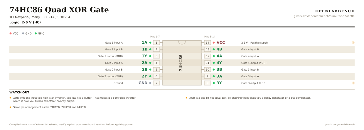
1.Pinout diagram
Highlight a signalhover to preview, click to keep
Pins 1-7
74HC86
Pins 8-14
Pin detail
Hover a pin for its mappings and gotchas. Click to keep it here.
- Logic level
- 2-6 V (HC)
- Package
- PDIP-14 / SOIC-14
Fig. 1. 74HC86 Quad XOR Gate, PDIP-14. Hover or tap a signal to light up every pin that carries it.
2.Watch out
- XOR with one input tied high is an inverter, tied low it is a buffer. That makes it a controlled inverter, which is how you build a selectable-polarity output.
- XOR is a one-bit not-equal test, so chaining them gives you a parity generator or a bus comparator.
- Same pin arrangement as the 74HC00, 74HC08 and 74HC32.
- HC inputs need a level near their own rail. Driving a 5 V part from 3.3 V logic wants the HCT version.
3.Controlled inverter
What has to go around the chip before it will run.
| Part | Between | Why |
|---|---|---|
| Wire link | 1B (2) to VCC | With one input high the XOR inverts the other. Drive this pin instead and you can switch inversion on and off. |
| Wire link | 4A (12) to GND | An unused input still has to be tied to a rail. |
| Wire link | 4B (13) to GND | The other input of the same unused gate. |
| 100 nF | VCC (14) to GND | Supply decoupling at the pin. |
A switchable inverter is most of why an XOR is on a board at all, that and parity. Four of them in a row make a one-instruction NOT across a nibble.
4.Full pin reference
Every pin, alias and mapping. This is the table that prints.
Table 2. Pin assignments.
| Pin | Name | Also called | Functions | Notes |
|---|---|---|---|---|
| 1 | 1A | - | Gate 1 input A | |
| 2 | 1B | - | Gate 1 input B | |
| 3 | 1Y | - | Gate 1 output (XOR) | |
| 4 | 2A | - | Gate 2 input A | |
| 5 | 2B | - | Gate 2 input B | |
| 6 | 2Y | - | Gate 2 output (XOR) | |
| 7 | GND | - | Ground | |
| 8 | 3Y | - | Gate 3 output (XOR) | Output comes first on this side. |
| 9 | 3A | - | Gate 3 input A | |
| 10 | 3B | - | Gate 3 input B | |
| 11 | 4Y | - | Gate 4 output (XOR) | |
| 12 | 4A | - | Gate 4 input A | |
| 13 | 4B | - | Gate 4 input B | |
| 14 | VCC2-6 V | - | Positive supply | 100 nF at the pin. |
Primary sources
Found a wrong pin? The whole board is one file, data/boards/sn74hc86.json.