Generic / WeAct · Dev board
STM32F103C8T6 Blue Pill
72 MHz Cortex-M3 with real SWD debugging for about the price of a Nano. Orientation below has the USB connector at the top.
- Logic level
- 3.3 V
- Package
- 2x20 2.54 mm, 53 x 22 mm
1.Pinout diagram
Highlight a signalhover to preview, click to keep
Header 1, USB at top
Header 2, USB at top
Pin detail
Hover a pin for its mappings and gotchas. Click to keep it here.
- Logic level
- 3.3 V
- Package
- 2x20 2.54 mm, 53 x 22 mm
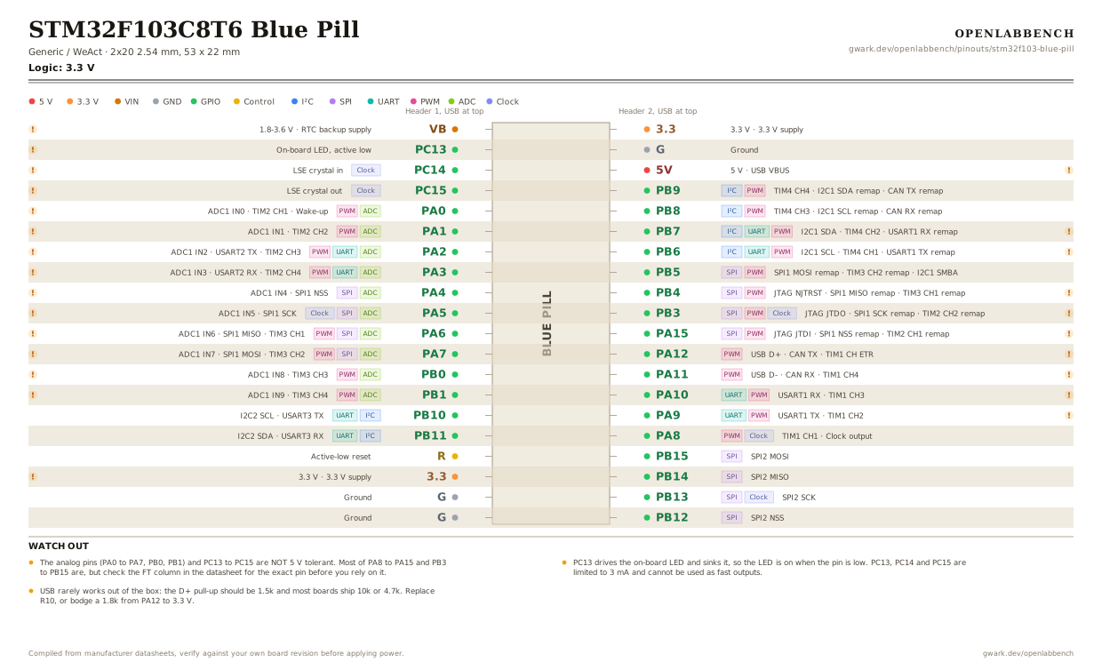
Fig. 1. STM32F103C8T6 Blue Pill, 2x20 2.54 mm, 53 x 22 mm. Hover or tap a signal to light up every pin that carries it.
2.Watch out
- The analog pins (PA0 to PA7, PB0, PB1) and PC13 to PC15 are NOT 5 V tolerant. Most of PA8 to PA15 and PB3 to PB15 are, but check the FT column in the datasheet for the exact pin before you rely on it.
- PC13 drives the on-board LED and sinks it, so the LED is on when the pin is low. PC13, PC14 and PC15 are limited to 3 mA and cannot be used as fast outputs.
- USB rarely works out of the box: the D+ pull-up should be 1.5k and most boards ship 10k or 4.7k. Replace R10, or bodge a 1.8k from PA12 to 3.3 V.
- PA13 and PA14 are SWDIO and SWCLK on the 4-pin debug header, not on the side headers. That header is the reason to pick this board: real breakpoints over a 3 dollar ST-Link clone.
- PA15, PB3 and PB4 default to JTAG. They need the JTAG remap disabled in software before they work as ordinary GPIO.
- BOOT0 high at reset runs the built-in serial bootloader on PA9/PA10. BOOT0 low runs your code. Move the jumper back after flashing or the next power cycle sits in the bootloader.
- The 5V header pin is wired straight to USB VBUS with no protection. Do not feed it from a bench supply with USB also plugged in.
- Plenty of boards in circulation carry a CKS or CS32 die rather than a real ST part. They mostly work, but SWD connection and USB behave differently, and the 128 KB flash on a C8-marked chip is unofficial.
3.Register configuration
Turning a pin on the diagram into a configured pin.
Blink the on-board LED on PC13
CMSIS, no HAL
#include "stm32f1xx.h"

/* 1. Clock the port. Nothing else works until this line runs. */
RCC->APB2ENR |= RCC_APB2ENR_IOPCEN;

/* 2. Configure PC13. Pins 8-15 live in CRH, 4 bits each,
      so PC13 sits at bit (13 - 8) * 4 = 20.
      MODE = 10 (output, 2 MHz), CNF = 00 (push-pull). */
GPIOC->CRH &= ~(0xFu << 20);
GPIOC->CRH |=  (0x2u << 20);

/* 3. BSRR writes without a read-modify-write, so it is
      interrupt-safe. The LED is active low on this board. */
GPIOC->BSRR = GPIO_BSRR_BR13;   /* LED on  */
GPIOC->BSRR = GPIO_BSRR_BS13;   /* LED off */
The peripheral clock enable in RCC is the step everyone misses. Without it the GPIO registers read and write as zero and the pin simply never moves, with no error anywhere.
4.Full pin reference
Every pin, alias and mapping. This is the table that prints.
Table 1. Pin assignments.
| Pin | Name | Also called | Functions | Notes |
|---|---|---|---|---|
| - | VB1.8-3.6 V | VBAT | RTC backup supply | No backup cell fitted. Tie to 3.3 V if unused. |
| - | PC13 | C13, LED_BUILTIN | On-board LED, active low | 3 mA max and slow. Fine for an LED, wrong for anything else. |
| - | PC14Clock | C14, OSC32_IN | LSE crystal in | 3 mA max. Taken by the 32.768 kHz crystal on most boards. |
| - | PC15Clock | C15, OSC32_OUT | LSE crystal out | 3 mA max. Taken by the 32.768 kHz crystal on most boards. |
| - | PA0ADCPWM | A0, ADC_IN0, WKUP | ADC1 IN0, TIM2 CH1, Wake-up | Not 5 V tolerant. |
| - | PA1ADCPWM | A1, ADC_IN1 | ADC1 IN1, TIM2 CH2 | Not 5 V tolerant. |
| - | PA2ADCUARTPWM | A2, ADC_IN2 | ADC1 IN2, USART2 TX, TIM2 CH3 | Not 5 V tolerant. |
| - | PA3ADCUARTPWM | A3, ADC_IN3 | ADC1 IN3, USART2 RX, TIM2 CH4 | Not 5 V tolerant. |
| - | PA4ADCSPI | A4, ADC_IN4 | ADC1 IN4, SPI1 NSS | Not 5 V tolerant. |
| - | PA5ADCSPIClock | A5, ADC_IN5 | ADC1 IN5, SPI1 SCK | Not 5 V tolerant. |
| - | PA6ADCSPIPWM | A6, ADC_IN6 | ADC1 IN6, SPI1 MISO, TIM3 CH1 | Not 5 V tolerant. |
| - | PA7ADCSPIPWM | A7, ADC_IN7 | ADC1 IN7, SPI1 MOSI, TIM3 CH2 | Not 5 V tolerant. |
| - | PB0ADCPWM | B0, ADC_IN8 | ADC1 IN8, TIM3 CH3 | Not 5 V tolerant. |
| - | PB1ADCPWM | B1, ADC_IN9 | ADC1 IN9, TIM3 CH4 | Not 5 V tolerant. |
| - | PB10I²CUART | B10 | I2C2 SCL, USART3 TX | |
| - | PB11I²CUART | B11 | I2C2 SDA, USART3 RX | |
| - | R | NRST, RESET | Active-low reset | |
| - | 3.33.3 V | - | 3.3 V supply | Also an input if you feed the board from a regulated 3.3 V rail. |
| - | G | - | Ground | |
| - | G | - | Ground | |
| - | 3.33.3 V | - | 3.3 V supply | |
| - | G | - | Ground | |
| - | 5V5 V | - | USB VBUS | Straight to the USB connector, unprotected and unfused. |
| - | PB9I²CPWM | B9 | TIM4 CH4, I2C1 SDA remap, CAN TX remap | |
| - | PB8I²CPWM | B8 | TIM4 CH3, I2C1 SCL remap, CAN RX remap | |
| - | PB7I²CUARTPWM | B7 | I2C1 SDA, TIM4 CH2, USART1 RX remap | Default I2C1 data pin. |
| - | PB6I²CUARTPWM | B6 | I2C1 SCL, TIM4 CH1, USART1 TX remap | Default I2C1 clock pin. |
| - | PB5SPIPWM | B5 | SPI1 MOSI remap, TIM3 CH2 remap, I2C1 SMBA | |
| - | PB4SPIPWM | B4, NJTRST | JTAG NJTRST, SPI1 MISO remap, TIM3 CH1 remap | JTAG by default. Disable the JTAG remap to use it as GPIO. |
| - | PB3SPIPWMClock | B3, JTDO | JTAG JTDO, SPI1 SCK remap, TIM2 CH2 remap | JTAG by default. Disable the JTAG remap to use it as GPIO. |
| - | PA15SPIPWM | A15, JTDI | JTAG JTDI, SPI1 NSS remap, TIM2 CH1 remap | JTAG by default. Disable the JTAG remap to use it as GPIO. |
| - | PA12PWM | A12, USB_DP | USB D+, CAN TX, TIM1 CH ETR | USB D+. This is the pin that needs the 1.5k pull-up to 3.3 V. |
| - | PA11PWM | A11, USB_DM | USB D-, CAN RX, TIM1 CH4 | USB D-. |
| - | PA10UARTPWM | A10 | USART1 RX, TIM1 CH3 | Serial bootloader RX when BOOT0 is high. |
| - | PA9UARTPWM | A9 | USART1 TX, TIM1 CH2 | Serial bootloader TX when BOOT0 is high. |
| - | PA8PWMClock | A8, MCO | TIM1 CH1, Clock output | |
| - | PB15SPI | B15 | SPI2 MOSI | |
| - | PB14SPI | B14 | SPI2 MISO | |
| - | PB13SPIClock | B13 | SPI2 SCK | |
| - | PB12SPI | B12 | SPI2 NSS |
Looking for a substitute?
Primary sources
Found a wrong pin? The whole board is one file, data/boards/stm32f103-blue-pill.json.