WeAct Studio · Dev board
STM32F411CEU6 Black Pill
100 MHz Cortex-M4F with USB-C that actually enumerates, the board most people move to after a Blue Pill. Pin 1 is top-left with USB-C up.
- Logic level
- 3.3 V
- Package
- 2x20 2.54 mm, 53 x 21 mm
1.Pinout diagram
Highlight a signalhover to preview, click to keep
Pins 1-20
Pins 21-40
Pin detail
Hover a pin for its mappings and gotchas. Click to keep it here.
- Logic level
- 3.3 V
- Package
- 2x20 2.54 mm, 53 x 21 mm
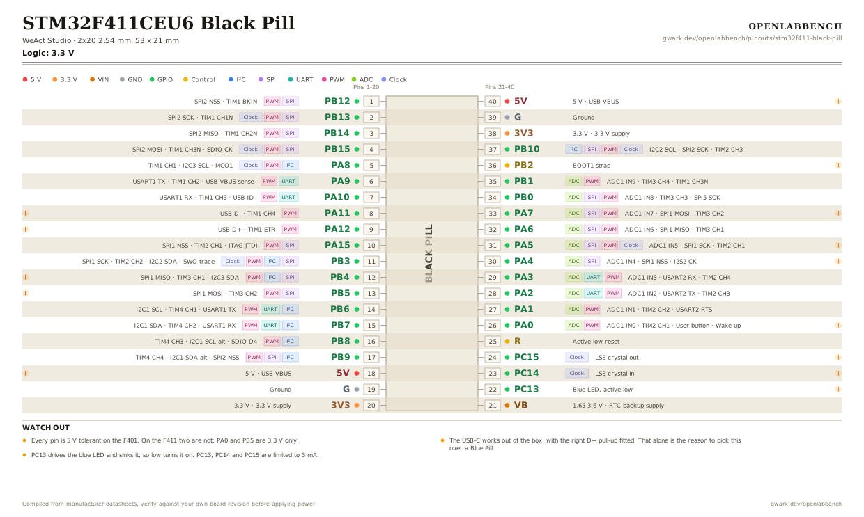
Fig. 1. STM32F411CEU6 Black Pill, 2x20 2.54 mm, 53 x 21 mm. Hover or tap a signal to light up every pin that carries it.
2.Watch out
- Every pin is 5 V tolerant on the F401. On the F411 two are not: PA0 and PB5 are 3.3 V only.
- The USB-C works out of the box, with the right D+ pull-up fitted. That alone is the reason to pick this over a Blue Pill.
- PC13 drives the blue LED and sinks it, so low turns it on. PC13, PC14 and PC15 are limited to 3 mA.
- There is a user button labeled KEY on PA0, active low, and it is already debounced in hardware. Holding BOOT0 at reset enters the built-in DFU bootloader over USB, so you can flash with dfu-util and no programmer at all.
- PA13 and PA14 are SWDIO and SWCLK on the 4-pin header at the bottom edge, not on the side headers.
- PA4, PA5, PA7 and PB4 also go to the optional on-board SPI flash footprint. If your board has the chip fitted, those four are shared.
- PB2 is BOOT1 and PC14 and PC15 carry the 32.768 kHz crystal, so treat all three as spoken for.
- The 5V header pins tie straight to USB VBUS with no protection. Do not back-feed them while USB is plugged in.
3.Register configuration
Turning a pin on the diagram into a configured pin.
Blink the on-board LED on PC13
CMSIS, no HAL
#include "stm32f4xx.h"

/* F4 is a different GPIO block from the F1. Clock gating moved to
   AHB1, and the four-bit CRL/CRH scheme is gone. */
RCC->AHB1ENR |= RCC_AHB1ENR_GPIOCEN;

/* MODER is 2 bits per pin: 01 = general purpose output. */
GPIOC->MODER &= ~(3u << (13 * 2));
GPIOC->MODER |=  (1u << (13 * 2));

GPIOC->OTYPER  &= ~(1u << 13);        /* push-pull */
GPIOC->OSPEEDR &= ~(3u << (13 * 2));  /* low speed is fine for an LED */

GPIOC->BSRR = GPIO_BSRR_BR13;         /* LED on, active low */
GPIOC->BSRR = GPIO_BSRR_BS13;         /* LED off */
Code written for an F1 Blue Pill will not compile here. CRL and CRH do not exist on the F4, the clock enable moved from APB2ENR to AHB1ENR, and MODER is two bits per pin instead of four.
4.Full pin reference
Every pin, alias and mapping. This is the table that prints.
Table 1. Pin assignments.
| Pin | Name | Also called | Functions | Notes |
|---|---|---|---|---|
| 1 | PB12SPIPWM | B12 | SPI2 NSS, TIM1 BKIN | |
| 2 | PB13SPIPWMClock | B13 | SPI2 SCK, TIM1 CH1N | |
| 3 | PB14SPIPWM | B14 | SPI2 MISO, TIM1 CH2N | |
| 4 | PB15SPIPWMClock | B15 | SPI2 MOSI, TIM1 CH3N, SDIO CK | |
| 5 | PA8I²CPWMClock | A8 | TIM1 CH1, I2C3 SCL, MCO1 | |
| 6 | PA9UARTPWM | A9 | USART1 TX, TIM1 CH2, USB VBUS sense | |
| 7 | PA10UARTPWM | A10 | USART1 RX, TIM1 CH3, USB ID | |
| 8 | PA11PWM | A11, USB_DM | USB D-, TIM1 CH4 | USB D-. |
| 9 | PA12PWM | A12, USB_DP | USB D+, TIM1 ETR | USB D+. |
| 10 | PA15SPIPWM | A15, JTDI | SPI1 NSS, TIM2 CH1, JTAG JTDI | |
| 11 | PB3SPII²CPWMClock | B3, JTDO, SWO | SPI1 SCK, TIM2 CH2, I2C2 SDA, SWO trace | |
| 12 | PB4SPII²CPWM | B4, NJTRST | SPI1 MISO, TIM3 CH1, I2C3 SDA | Shared with the optional on-board SPI flash. |
| 13 | PB5SPIPWM | B5 | SPI1 MOSI, TIM3 CH2 | Not 5 V tolerant on the F411. |
| 14 | PB6I²CUARTPWM | B6 | I2C1 SCL, TIM4 CH1, USART1 TX | |
| 15 | PB7I²CUARTPWM | B7 | I2C1 SDA, TIM4 CH2, USART1 RX | |
| 16 | PB8I²CPWM | B8 | TIM4 CH3, I2C1 SCL alt, SDIO D4 | |
| 17 | PB9I²CSPIPWM | B9 | TIM4 CH4, I2C1 SDA alt, SPI2 NSS | |
| 18 | 5V5 V | - | USB VBUS | Unprotected, straight to the connector. |
| 19 | G | GND | Ground | |
| 20 | 3V33.3 V | - | 3.3 V supply | |
| 21 | VB1.65-3.6 V | VBAT | RTC backup supply | |
| 22 | PC13 | C13, LED_BUILTIN | Blue LED, active low | 3 mA max. Fine for the LED, wrong for a load. |
| 23 | PC14Clock | C14, OSC32_IN | LSE crystal in | 3 mA max, and taken by the 32.768 kHz crystal. |
| 24 | PC15Clock | C15, OSC32_OUT | LSE crystal out | 3 mA max, and taken by the 32.768 kHz crystal. |
| 25 | R | NRST, RESET | Active-low reset | |
| 26 | PA0ADCPWM | A0, KEY, WKUP | ADC1 IN0, TIM2 CH1, User button, Wake-up | The KEY button, active low and hardware debounced. Not 5 V tolerant on the F411. |
| 27 | PA1ADCPWM | A1 | ADC1 IN1, TIM2 CH2, USART2 RTS | |
| 28 | PA2ADCUARTPWM | A2 | ADC1 IN2, USART2 TX, TIM2 CH3 | |
| 29 | PA3ADCUARTPWM | A3 | ADC1 IN3, USART2 RX, TIM2 CH4 | |
| 30 | PA4ADCSPI | A4 | ADC1 IN4, SPI1 NSS, I2S2 CK | Shared with the optional on-board SPI flash. |
| 31 | PA5ADCSPIPWMClock | A5 | ADC1 IN5, SPI1 SCK, TIM2 CH1 | Shared with the optional on-board SPI flash. |
| 32 | PA6ADCSPIPWM | A6 | ADC1 IN6, SPI1 MISO, TIM3 CH1 | |
| 33 | PA7ADCSPIPWM | A7 | ADC1 IN7, SPI1 MOSI, TIM3 CH2 | Shared with the optional on-board SPI flash. |
| 34 | PB0ADCSPIPWM | B0 | ADC1 IN8, TIM3 CH3, SPI5 SCK | |
| 35 | PB1ADCPWM | B1 | ADC1 IN9, TIM3 CH4, TIM1 CH3N | |
| 36 | PB2 | B2, BOOT1 | BOOT1 strap | Boot mode select. Usable as GPIO, but it is sampled at reset. |
| 37 | PB10I²CSPIPWMClock | B10 | I2C2 SCL, SPI2 SCK, TIM2 CH3 | |
| 38 | 3V33.3 V | - | 3.3 V supply | |
| 39 | G | GND | Ground | |
| 40 | 5V5 V | - | USB VBUS | Unprotected, straight to the connector. |
Primary sources
Found a wrong pin? The whole board is one file, data/boards/stm32f411-black-pill.json.