PJRC · Dev board
Teensy 4.1
A 600 MHz Cortex-M7 on a board the size of a stick of gum, with Ethernet pads, an SD socket and more serial ports than most people can use.
- Logic level
- 3.3 V, not 5 V tolerant
- Package
- 2x24 2.54 mm, 61 x 18 mm
1.Pinout diagram
Highlight a signalhover to preview, click to keep
Left (USB at top)
TEENSY 4.1
Right (USB at top)
Pin detail
Hover a pin for its mappings and gotchas. Click to keep it here.
- Logic level
- 3.3 V, not 5 V tolerant
- Package
- 2x24 2.54 mm, 61 x 18 mm
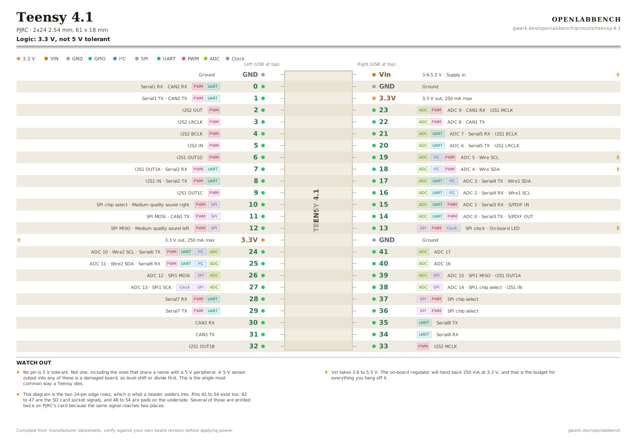
Fig. 1. Teensy 4.1, 2x24 2.54 mm, 61 x 18 mm. Hover or tap a signal to light up every pin that carries it.
2.Watch out
- No pin is 5 V tolerant. Not one, including the ones that share a name with a 5 V peripheral. A 5 V sensor output into any of these is a damaged board, so level shift or divide first. This is the single most common way a Teensy dies.
- Vin takes 3.6 to 5.5 V. The on-board regulator will hand back 250 mA at 3.3 V, and that is the budget for everything you hang off it.
- This diagram is the two 24-pin edge rows, which is what a header solders into. Pins 42 to 54 exist too: 42 to 47 are the SD card socket signals, and 48 to 54 are pads on the underside. Several of those are printed twice on PJRC's card because the same signal reaches two places.
- Also on the underside: VBAT for a coin cell that keeps the real-time clock running, pads for the Program and On/Off buttons, a 6-pin Ethernet connection, and footprints for extra flash and PSRAM.
- Pin 13 is the on-board LED as well as SPI SCK. Using hardware SPI makes the LED flicker with traffic, which is a free bus activity indicator and a nuisance in equal measure.
- Every digital pin can raise an interrupt, which is unusual and worth remembering before you go hunting for the special ones.
- Analog pins A0 to A17 are scattered: A0 to A9 sit on the right row around pins 14 to 23, A10 to A13 are on the left among 24 to 27, and A14 to A17 come back on the right at 38 to 41.
- The USB connector is at the top of this diagram. Turn the board over and the left column becomes the right one, which is how most miswiring starts.
3.Full pin reference
Every pin, alias and mapping. This is the table that prints.
Table 1. Pin assignments.
| Pin | Name | Also called | Functions | Notes |
|---|---|---|---|---|
| - | GND | - | Ground | |
| - | 0UARTPWM | RX1, CRX2, CS1 | Serial1 RX, CAN2 RX | |
| - | 1UARTPWM | TX1, CTX2, MISO1 | Serial1 TX, CAN2 TX | |
| - | 2PWM | OUT2 | I2S2 OUT | |
| - | 3PWM | LRCLK2 | I2S2 LRCLK | |
| - | 4PWM | BCLK2 | I2S2 BCLK | |
| - | 5PWM | IN2 | I2S2 IN | |
| - | 6PWM | OUT1D | I2S1 OUT1D | |
| - | 7UARTPWM | OUT1A, RX2 | I2S1 OUT1A, Serial2 RX | |
| - | 8UARTPWM | IN1, TX2 | I2S1 IN, Serial2 TX | |
| - | 9PWM | OUT1C | I2S1 OUT1C | |
| - | 10SPIPWM | MQSR, CS | SPI chip select, Medium quality sound right | |
| - | 11SPIPWM | MOSI, CTX1 | SPI MOSI, CAN1 TX | |
| - | 12SPIPWM | MISO, MQSL | SPI MISO, Medium quality sound left | |
| - | 3.3V | - | 3.3 V out, 250 mA max | Regulator output. Also the only safe level for any input pin. |
| - | 24ADCI²CUARTPWM | A10, SCL2, TX6 | ADC 10, Wire2 SCL, Serial6 TX | |
| - | 25ADCI²CUARTPWM | A11, SDA2, RX6 | ADC 11, Wire2 SDA, Serial6 RX | |
| - | 26ADCSPI | A12, MOSI1 | ADC 12, SPI1 MOSI | |
| - | 27ADCSPIClock | A13, SCK1 | ADC 13, SPI1 SCK | |
| - | 28UARTPWM | RX7 | Serial7 RX | |
| - | 29UARTPWM | TX7 | Serial7 TX | |
| - | 30 | CRX3 | CAN3 RX | |
| - | 31 | CTX3 | CAN3 TX | |
| - | 32 | OUT1B | I2S1 OUT1B | |
| - | Vin3.6-5.5 V | - | Supply in | Feed the board here, or from USB, but cut the VUSB pad before doing both. |
| - | GND | - | Ground | |
| - | 3.3V | - | 3.3 V out, 250 mA max | |
| - | 23ADCPWM | A9, CRX1, MCLK1 | ADC 9, CAN1 RX, I2S1 MCLK | |
| - | 22ADCPWM | A8, CTX1 | ADC 8, CAN1 TX | |
| - | 21ADCUART | A7, RX5, BCLK1 | ADC 7, Serial5 RX, I2S1 BCLK | |
| - | 20ADCUART | A6, TX5, LRCLK1 | ADC 6, Serial5 TX, I2S1 LRCLK | |
| - | 19ADCI²CPWM | A5, SCL | ADC 5, Wire SCL | The default I2C clock. Needs a pull-up; there is none on the board. |
| - | 18ADCI²CPWM | A4, SDA | ADC 4, Wire SDA | The default I2C data line. |
| - | 17ADCUARTI²C | A3, TX4, SDA1 | ADC 3, Serial4 TX, Wire1 SDA | |
| - | 16ADCUARTI²C | A2, RX4, SCL1 | ADC 2, Serial4 RX, Wire1 SCL | |
| - | 15ADCUARTPWM | A1, RX3 | ADC 1, Serial3 RX, S/PDIF IN | |
| - | 14ADCUARTPWM | A0, TX3 | ADC 0, Serial3 TX, S/PDIF OUT | |
| - | 13SPIPWMClock | LED, SCK | SPI clock, On-board LED | On-board LED. It blinks with SPI traffic whether you want it to or not. |
| - | GND | - | Ground | |
| - | 41ADC | A17 | ADC 17 | |
| - | 40ADC | A16 | ADC 16 | |
| - | 39ADCSPI | A15, MISO1, OUT1A | ADC 15, SPI1 MISO, I2S1 OUT1A | |
| - | 38ADCSPI | A14, CS1, IN1 | ADC 14, SPI1 chip select, I2S1 IN | |
| - | 37SPIPWM | CS | SPI chip select | |
| - | 36SPIPWM | CS | SPI chip select | |
| - | 35UART | TX8 | Serial8 TX | |
| - | 34UART | RX8 | Serial8 RX | |
| - | 33PWM | MCLK2 | I2S2 MCLK |
Primary sources
Found a wrong pin? The whole board is one file, data/boards/teensy-4-1.json.