TI / ST / Toshiba · Integrated circuit
ULN2003 Darlington Array
Seven open-collector Darlington sinks with built-in clamp diodes, for relays, solenoids and 28BYJ-48 steppers.
- Logic level
- Inputs 5 V TTL, outputs to 50 V
- Package
- PDIP-16 / SOIC-16
1.Pinout diagram
Highlight a signalhover to preview, click to keep
Pins 1-8
ULN2003
Pins 9-16
Pin detail
Hover a pin for its mappings and gotchas. Click to keep it here.
- Logic level
- Inputs 5 V TTL, outputs to 50 V
- Package
- PDIP-16 / SOIC-16
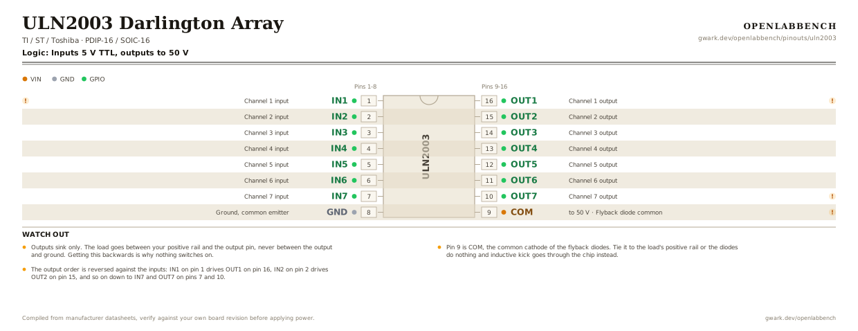
Fig. 1. ULN2003 Darlington Array, PDIP-16. Hover or tap a signal to light up every pin that carries it.
2.Watch out
- Outputs sink only. The load goes between your positive rail and the output pin, never between the output and ground. Getting this backwards is why nothing switches on.
- Pin 9 is COM, the common cathode of the flyback diodes. Tie it to the load's positive rail or the diodes do nothing and inductive kick goes through the chip instead.
- The output order is reversed against the inputs: IN1 on pin 1 drives OUT1 on pin 16, IN2 on pin 2 drives OUT2 on pin 15, and so on down to IN7 and OUT7 on pins 7 and 10.
- 500 mA per channel, but not on all seven at once. The package dissipation limit lands around 1.5 W total, so a full load of seven relays will overheat it.
- Darlington saturation drop is about 1 V at 350 mA, wasted as heat. The TBD62083A is pin compatible, DMOS, and drops a third of a volt.
- ULN2003 inputs are sized for 5 V logic. ULN2004 is the same part with input resistors for 6 to 15 V CMOS.
- For eight channels use the ULN2803, which is DIP-18 with a different pinout rather than a wider version of this one.
3.Driving an inductive load
What has to go around the chip before it will run.
| Part | Between | Why |
|---|---|---|
| Wire link | COM (9) to VCC | Connects the internal clamp diodes to the load's rail. Without it the flyback goes through the chip. |
| Load | COM (9) to OUT1 (16) | Coil or solenoid from the positive rail to an output. The outputs sink only. |
500 mA per channel, but not on all seven at once. Package dissipation caps the total around 1.5 W.
4.Full pin reference
Every pin, alias and mapping. This is the table that prints.
Table 2. Pin assignments.
| Pin | Name | Also called | Functions | Notes |
|---|---|---|---|---|
| 1 | IN1 | 1B | Channel 1 input | Drives OUT1 on pin 16. |
| 2 | IN2 | 2B | Channel 2 input | |
| 3 | IN3 | 3B | Channel 3 input | |
| 4 | IN4 | 4B | Channel 4 input | |
| 5 | IN5 | 5B | Channel 5 input | |
| 6 | IN6 | 6B | Channel 6 input | |
| 7 | IN7 | 7B | Channel 7 input | |
| 8 | GND | E | Ground, common emitter | |
| 9 | COMto 50 V | - | Flyback diode common | Connect to the load's supply rail. Without it the clamp diodes are not in circuit. |
| 10 | OUT7 | 7C | Channel 7 output | Open collector sink, 500 mA. |
| 11 | OUT6 | 6C | Channel 6 output | |
| 12 | OUT5 | 5C | Channel 5 output | |
| 13 | OUT4 | 4C | Channel 4 output | |
| 14 | OUT3 | 3C | Channel 3 output | |
| 15 | OUT2 | 2C | Channel 2 output | |
| 16 | OUT1 | 1C | Channel 1 output | Driven by IN1 on pin 1, at the opposite corner. |
Looking for a substitute?
Primary sources
Found a wrong pin? The whole board is one file, data/boards/uln2003.json.