WEMOS / LOLIN · Dev board
WEMOS D1 mini (ESP8266)
ESP8266 WiFi board in a 34 x 25 mm footprint. Only one ADC and a handful of usable GPIO, several of which are boot strapping pins, the constraint that defines most D1 mini projects.
- Logic level
- 3.3 V
- Package
- 2x8 2.54 mm, 34.2 x 25.6 mm
1.Pinout diagram
Highlight a signalhover to preview, click to keep
Left (USB at bottom)
D1 MINI
Right (USB at bottom)
Pin detail
Hover a pin for its mappings and gotchas. Click to keep it here.
- Logic level
- 3.3 V
- Package
- 2x8 2.54 mm, 34.2 x 25.6 mm
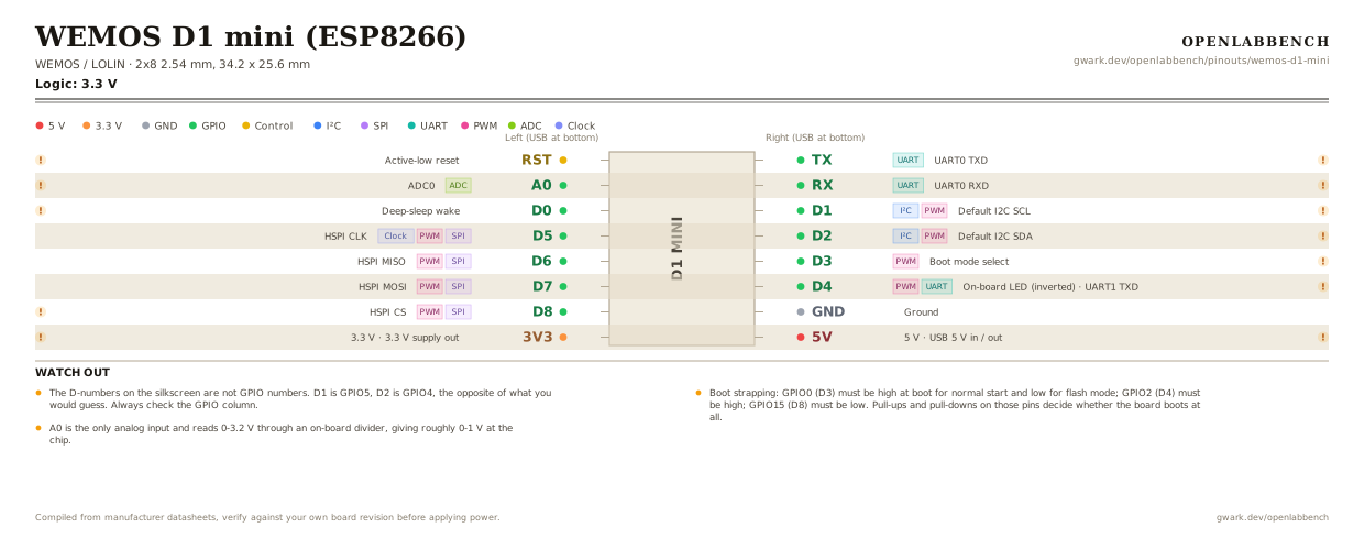
Fig. 1. WEMOS D1 mini (ESP8266), 2x8 2.54 mm, 34.2 x 25.6 mm. Hover or tap a signal to light up every pin that carries it.
2.Watch out
- The D-numbers on the silkscreen are not GPIO numbers. D1 is GPIO5, D2 is GPIO4, the opposite of what you would guess. Always check the GPIO column.
- Boot strapping: GPIO0 (D3) must be high at boot for normal start and low for flash mode; GPIO2 (D4) must be high; GPIO15 (D8) must be low. Pull-ups and pull-downs on those pins decide whether the board boots at all.
- A0 is the only analog input and reads 0-3.2 V through an on-board divider, giving roughly 0-1 V at the chip.
- GPIO16 (D0) comes off a different peripheral block: no interrupts, no PWM, no I2C, and it has a weak internal pull-down rather than a pull-up. It is the pin that wakes the chip from deep sleep when tied to RST.
- I2C is done in software on the ESP8266, so SDA/SCL can be any usable GPIO; D1/D2 are only the Arduino core defaults.
- Pins are 3.3 V and not 5 V tolerant, though the 5V pin passes USB power straight through for peripherals.
3.Full pin reference
Every pin, alias and mapping. This is the table that prints.
Table 1. Pin assignments.
| Pin | Name | Also called | Functions | Notes |
|---|---|---|---|---|
| - | RST | RESET | Active-low reset | Tie to D0 (GPIO16) to wake from deep sleep. |
| - | A0ADC | ADC0, TOUT | ADC0 | 0-3.2 V input range through an on-board divider. 10-bit. |
| - | D0 | GPIO16 | Deep-sleep wake | No interrupt, no PWM, no I2C. Internal pull-down only. |
| - | D5SPIPWMClock | GPIO14, SCLK | HSPI CLK | |
| - | D6SPIPWM | GPIO12, MISO | HSPI MISO | |
| - | D7SPIPWM | GPIO13, MOSI | HSPI MOSI | |
| - | D8SPIPWM | GPIO15, CS | HSPI CS | Strapping pin: must be low at boot. Has a 10k pull-down on board. |
| - | 3V33.3 V | - | 3.3 V supply out | ~500 mA from the on-board regulator, minus what the radio draws in bursts. |
| - | TXUART | GPIO1, D10, TXD0 | UART0 TXD | Shared with the USB bridge and the boot log. |
| - | RXUART | GPIO3, D9, RXD0 | UART0 RXD | Shared with the USB bridge. |
| - | D1I²CPWM | GPIO5, SCL | Default I2C SCL | One of the two safest general-purpose pins, no strapping role. |
| - | D2I²CPWM | GPIO4, SDA | Default I2C SDA | The other safe general-purpose pin. |
| - | D3PWM | GPIO0, FLASH | Boot mode select | Strapping pin: high to boot, low for flash mode. Has a 10k pull-up; a button to GND is fine, a steady load is not. |
| - | D4PWMUART | GPIO2, LED_BUILTIN, TXD1 | On-board LED (inverted), UART1 TXD | Strapping pin: must be high at boot. LED is active-low. |
| - | GND | - | Ground | |
| - | 5V5 V | - | USB 5 V in / out | Straight to the micro-USB rail. Usable as a 5 V input to power the board. |
Looking for a substitute?
Primary sources
Found a wrong pin? The whole board is one file, data/boards/wemos-d1-mini.json.