Seeed Studio · Dev board
Seeed XIAO ESP32C3
A thumbnail-sized RISC-V board with WiFi, BLE and a battery charger. The 14-pin XIAO footprint is shared across the whole family, so a SAMD21, RP2040 or nRF52840 drops into the same socket. USB-C at the top.
- Logic level
- 3.3 V
- Package
- 2x7 2.54 mm, 21 x 17.5 mm
1.Pinout diagram
Highlight a signalhover to preview, click to keep
Left (USB-C at top)
Right (USB-C at top)
Pin detail
Hover a pin for its mappings and gotchas. Click to keep it here.
- Logic level
- 3.3 V
- Package
- 2x7 2.54 mm, 21 x 17.5 mm
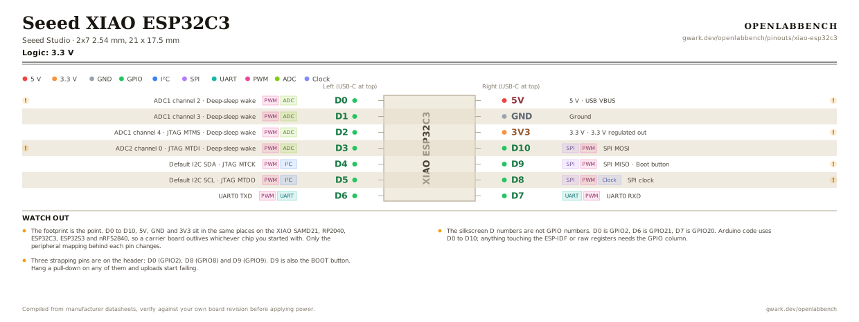
Fig. 1. Seeed XIAO ESP32C3, 2x7 2.54 mm, 21 x 17.5 mm. Hover or tap a signal to light up every pin that carries it.
2.Watch out
- The footprint is the point. D0 to D10, 5V, GND and 3V3 sit in the same places on the XIAO SAMD21, RP2040, ESP32C3, ESP32S3 and nRF52840, so a carrier board outlives whichever chip you started with. Only the peripheral mapping behind each pin changes.
- The silkscreen D numbers are not GPIO numbers. D0 is GPIO2, D6 is GPIO21, D7 is GPIO20. Arduino code uses D0 to D10; anything touching the ESP-IDF or raw registers needs the GPIO column.
- Three strapping pins are on the header: D0 (GPIO2), D8 (GPIO8) and D9 (GPIO9). D9 is also the BOOT button. Hang a pull-down on any of them and uploads start failing.
- Four analog inputs, D0 to D3, but only D0 to D2 are on ADC1. D3 is ADC2, which the radio takes over, so an analog read there stops working once WiFi is up.
- There is a lithium battery charger on board, with pads on the underside rather than a connector. The charge LED is on its own pin, not a GPIO.
- 5V is VBUS, straight from the USB connector. It is an input when you power the board that way and an output when USB is connected, and it is not regulated.
- Only D0 to D3 can wake the chip from deep sleep.
- There is a U.FL connector for an external antenna next to the PCB trace antenna. A solder jumper selects between them; moving it is worth several dB.
- Adafruit's QT Py uses this same 14-pin footprint, so the two are interchangeable in a carrier. The larger Adafruit Feather footprint is a different thing entirely and FeatherWings will not fit.
3.Register configuration
Turning a pin on the diagram into a configured pin.
Drive a pin and read an analog input
ESP-IDF v5
#include "driver/gpio.h"
#include "esp_adc/adc_oneshot.h"

/* Silkscreen D numbers are not GPIO numbers: D0 is GPIO2. */
gpio_reset_pin(GPIO_NUM_2);
gpio_set_direction(GPIO_NUM_2, GPIO_MODE_OUTPUT);
gpio_set_level(GPIO_NUM_2, 1);

adc_oneshot_unit_handle_t adc1;
adc_oneshot_unit_init_cfg_t unit = { .unit_id = ADC_UNIT_1 };
adc_oneshot_new_unit(&unit, &adc1);

adc_oneshot_chan_cfg_t ch = {
    .atten    = ADC_ATTEN_DB_12,   /* full 0 to ~3.1 V range */
    .bitwidth = ADC_BITWIDTH_DEFAULT,
};
adc_oneshot_config_channel(adc1, ADC_CHANNEL_2, &ch);   /* GPIO2 = D0 */

int raw;
adc_oneshot_read(adc1, ADC_CHANNEL_2, &raw);
Only D0 to D2 are on ADC1. D3 is ADC2, which the WiFi driver takes over, so a read there starts failing the moment the radio connects.
4.Full pin reference
Every pin, alias and mapping. This is the table that prints.
Table 1. Pin assignments.
| Pin | Name | Also called | Functions | Notes |
|---|---|---|---|---|
| - | D0ADCPWM | GPIO2, A0, ADC1_CH2 | ADC1 channel 2, Deep-sleep wake | Strapping pin. Also the usual place to hang a battery voltage divider. |
| - | D1ADCPWM | GPIO3, A1, ADC1_CH3 | ADC1 channel 3, Deep-sleep wake | |
| - | D2ADCPWM | GPIO4, A2, ADC1_CH4 | ADC1 channel 4, JTAG MTMS, Deep-sleep wake | |
| - | D3ADCPWM | GPIO5, A3, ADC2_CH0 | ADC2 channel 0, JTAG MTDI, Deep-sleep wake | ADC2, which the radio takes over. Analog reads here stop working once WiFi is connected. |
| - | D4I²CPWM | GPIO6, SDA | Default I2C SDA, JTAG MTCK | |
| - | D5I²CPWM | GPIO7, SCL | Default I2C SCL, JTAG MTDO | |
| - | D6UARTPWM | GPIO21, TX, U0TXD | UART0 TXD | |
| - | 5V5 V | - | USB VBUS | Unregulated, straight to the USB connector. Input or output depending on how the board is powered. |
| - | GND | - | Ground | |
| - | 3V33.3 V | - | 3.3 V regulated out | Output from the on-board regulator, about 700 mA before the radio takes its share. |
| - | D10SPIPWM | GPIO10, MOSI | SPI MOSI | |
| - | D9SPIPWM | GPIO9, MISO, BOOT | SPI MISO, Boot button | Strapping pin and the BOOT button. Pulling it low at reset enters the bootloader. |
| - | D8SPIPWMClock | GPIO8, SCK | SPI clock | Strapping pin: must be high at boot. |
| - | D7UARTPWM | GPIO20, RX, U0RXD | UART0 RXD |
Primary sources
Found a wrong pin? The whole board is one file, data/boards/xiao-esp32c3.json.