Zilog · Microcontroller
Zilog Z80
8-bit CPU of the ZX Spectrum, MSX and CP/M era, with a scattered data bus that catches everyone wiring one by hand.
- Logic level
- 5 V
- Package
- PDIP-40
1.Pinout diagram
Highlight a signalhover to preview, click to keep
Pins 1-20
Z80
Pins 21-40
Pin detail
Hover a pin for its mappings and gotchas. Click to keep it here.
- Logic level
- 5 V
- Package
- PDIP-40
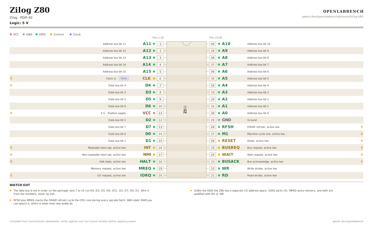
Fig. 1. Zilog Z80, PDIP-40. Hover or tap a signal to light up every pin that carries it.
2.Watch out
- The data bus is not in order on the package: pins 7 to 15 run D4, D3, D5, D6, VCC, D2, D7, D0, D1. Wire it from the numbers, never by eye.
- Unlike the 6502 the Z80 has a separate I/O address space. IORQ picks I/O, MREQ picks memory, and both are qualified with RD or WR.
- RFSH plus MREQ marks the DRAM refresh cycle the CPU runs during every opcode fetch. With static RAM you can ignore it, which is what most new builds do.
- M1 low marks an opcode fetch. M1 with IORQ is the interrupt acknowledge cycle, not an I/O read.
- RESET must be held low for at least three full clock cycles. The CPU then starts at address 0000.
- The CPU needs a single phase clock with a fast rise time and, on the original NMOS part, a pull-up to get near 5 V. The CMOS Z84C00 is happier with ordinary logic and is fully static, so you can single-step it.
- BUSREQ and BUSACK give you real DMA, and WAIT lets slow memory stretch a cycle. Tie INT, NMI, WAIT and BUSREQ high through resistors if you are not using them.
3.Minimum circuit to run
What has to go around the chip before it will run.
| Part | Between | Why |
|---|---|---|
| Clock oscillator | CLK (6) to GND | A single-phase 5 V clock. The NMOS part also has a minimum clock speed, so it cannot be single-stepped slowly. |
| 330 Ohmoptional | CLK (6) to VCC | The NMOS Z80 wants the clock pulled close to VCC. CMOS parts, the Z84C00, do not need this. |
| 10 kOhm | RESET (26) to VCC | Reset pull-up, with a capacitor to ground for a power-on reset of at least three clocks. |
| 10 uF | RESET (26) to GND | Holds RESET low while the supply comes up. |
| 10 kOhm | INT (16) to VCC | An unused interrupt input must be held high or you take interrupts that never happened. |
| 10 kOhm | NMI (17) to VCC | NMI is edge triggered and cannot be masked, so a floating pin is worse than a floating INT. |
| 10 kOhm | WAIT (24) to VCC | WAIT held low stretches every machine cycle forever. The bus simply stops. |
| 10 kOhm | BUSREQ (25) to VCC | BUSREQ held low floats the address and data buses and hands them to nobody. |
| 100 nF | VCC (11) to GND | Supply decoupling at the pin. |
Qualify memory and I/O decoding with MREQ (19) and IORQ (20). The Z80 puts the refresh address on A0-A6 during the second half of every M1 cycle, so raw address lines are not a valid chip select.
4.Full pin reference
Every pin, alias and mapping. This is the table that prints.
Table 2. Pin assignments.
| Pin | Name | Also called | Functions | Notes |
|---|---|---|---|---|
| 1 | A11 | - | Address bus bit 11 | |
| 2 | A12 | - | Address bus bit 12 | |
| 3 | A13 | - | Address bus bit 13 | |
| 4 | A14 | - | Address bus bit 14 | |
| 5 | A15 | - | Address bus bit 15 | |
| 6 | CLKClock | - | Clock in | Single phase. The NMOS part wants a pull-up to reach a valid high. |
| 7 | D4 | - | Data bus bit 4 | The data bus order on the package is scrambled. Start here. |
| 8 | D3 | - | Data bus bit 3 | |
| 9 | D5 | - | Data bus bit 5 | |
| 10 | D6 | - | Data bus bit 6 | |
| 11 | VCC5 V | - | Positive supply | Sits in the middle of the data bus, not at a corner. |
| 12 | D2 | - | Data bus bit 2 | |
| 13 | D7 | - | Data bus bit 7 | |
| 14 | D0 | - | Data bus bit 0 | |
| 15 | D1 | - | Data bus bit 1 | |
| 16 | INT | - | Maskable interrupt, active low | Sampled at the end of an instruction. Tie high if unused. |
| 17 | NMI | - | Non-maskable interrupt, active low | Edge triggered, vectors to 0066. Tie high if unused. |
| 18 | HALT | - | Halt state, active low | The CPU executes NOPs until an interrupt arrives. |
| 19 | MREQ | - | Memory request, active low | |
| 20 | IORQ | - | I/O request, active low | With M1 this is an interrupt acknowledge, not an I/O cycle. |
| 21 | RD | - | Read strobe, active low | |
| 22 | WR | - | Write strobe, active low | |
| 23 | BUSACK | BUSAK | Bus acknowledge, active low | Address, data and control go high impedance while this is low. |
| 24 | WAIT | - | Wait request, active low | Hold low to stretch the current cycle for slow memory. Tie high if unused. |
| 25 | BUSREQ | BUSRQ | Bus request, active low | Tie high if unused. |
| 26 | RESET | - | Reset, active low | Hold low for at least three clock cycles. Starts execution at 0000. |
| 27 | M1 | - | Machine cycle one, active low | Low during an opcode fetch. |
| 28 | RFSH | - | DRAM refresh, active low | Ignorable with static RAM. |
| 29 | GND | - | Ground | |
| 30 | A0 | - | Address bus bit 0 | |
| 31 | A1 | - | Address bus bit 1 | |
| 32 | A2 | - | Address bus bit 2 | |
| 33 | A3 | - | Address bus bit 3 | |
| 34 | A4 | - | Address bus bit 4 | |
| 35 | A5 | - | Address bus bit 5 | |
| 36 | A6 | - | Address bus bit 6 | |
| 37 | A7 | - | Address bus bit 7 | |
| 38 | A8 | - | Address bus bit 8 | |
| 39 | A9 | - | Address bus bit 9 | |
| 40 | A10 | - | Address bus bit 10 |
Looking for a substitute?
Primary sources
Found a wrong pin? The whole board is one file, data/boards/zilog-z80.json.